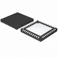
MAX9856ETL+ Maxim Integrated Products, MAX9856ETL+ Datasheet - Page 2

MAX9856ETL+
Manufacturer Part Number
MAX9856ETL+
Description
IC CODEC AUDIO LP 40TQFN-EP
Manufacturer
Maxim Integrated Products
Type
Audio Codecr
Datasheet
1.MAX9856ETL.pdf
(46 pages)
Specifications of MAX9856ETL+
Data Interface
Serial
Resolution (bits)
18 b
Number Of Adcs / Dacs
2 / 2
Sigma Delta
Yes
S/n Ratio, Adcs / Dacs (db) Typ
77 / 91
Dynamic Range, Adcs / Dacs (db) Typ
85 / 91
Voltage - Supply, Analog
1.71 V ~ 3.6 V
Voltage - Supply, Digital
1.71 V ~ 3.6 V
Operating Temperature
-40°C ~ 85°C
Mounting Type
Surface Mount
Package / Case
40-WFQFN Exposed Pad
Number Of Adc Inputs
2
Number Of Dac Outputs
2
Interface Type
I2C
Resolution
18 bit
Operating Supply Voltage
1.71 V to 3.6 V
Maximum Operating Temperature
+ 85 C
Mounting Style
SMD/SMT
Minimum Operating Temperature
- 40 C
Supply Current
2.9 mA
Thd Plus Noise
82 dB
Audio Codec Type
Stereo
No. Of Adcs
2
No. Of Dacs
2
No. Of Input Channels
2
No. Of Output Channels
2
Adc / Dac Resolution
18bit
Adcs / Dacs Signal To Noise Ratio
91dB
Rohs Compliant
Yes
Lead Free Status / RoHS Status
Lead free / RoHS Compliant
Low-Power Audio CODEC with
DirectDrive Headphone Amplifiers
ABSOLUTE MAXIMUM RATINGS
(Voltages with respect to AGND.)
AVDD, DVDD, DVDDS2, CPVDD .............................-0.3V to +4V
PVSS, SVSS........................................Capacitor connection only
AGND, DGND, CPGND.........................................-0.3V to +0.3V
HPL, HPR ...................................(SVSS - 0.3V) to (AVDD + 0.3V)
HGNDSNS, LGNDSNS, MICGND .........................-0.3V to +0.3V
JACKSNS ...................................(SVSS - 0.3V) to (AVDD + 0.3V)
LOUTL, LOUTR ..........................(SVSS - 0.3V) to (AVDD + 0.3V)
LINEIN1, LINEIN2, AUXIN ...........................................-2V to +2V
MICL, MICR, INLP, INLM, INRM..................................-2V to +2V
C1N .........................................(PVSS - 0.3V) to (CPGND + 0.3V)
C1P ......................................(CPGND - 0.3V) to (CPVDD + 0.3V)
PREG, REF, MBIAS, MICBIAS.................-0.3V to (AVDD + 0.3V)
NREG .......................................................(SVSS - 0.3V) to +0.3V
MCLK........................................................................-0.3V to +4V
SDA, SCL, IRQ .........................................................-0.3V to +4V
ELECTRICAL CHARACTERISTICS
(V
C
otherwise noted. Typical values are at T
Stresses beyond those listed under “Absolute Maximum Ratings” may cause permanent damage to the device. These are stress ratings only, and functional
operation of the device at these or any other conditions beyond those indicated in the operational sections of the specifications is not implied. Exposure to
absolute maximum rating conditions for extended periods may affect device reliability.
2
Supply Voltage Range
Total Supply Current (Note 2)
Shutdown Supply Current
Shutdown to Full Operation
NREG
AVDD
_______________________________________________________________________________________
= 1µF, A
= V
PARAMETER
CPVDD
VPRE
= V
= +20dB, C
DVDDS2
= V
MICBIAS
DVDD
SYMBOL
A
I
VDD
= 1.8V, R
= +25°C.) (Note 1)
= 1µF, A
AVDD = CPVDD (inferred from HP output
PSRR)
DVDD, DVDDS2 (inferred from CODEC
performance tests)
DAC playback mode
(f
Line-only playback mode
(DAC/ADC disabled)
DAC + line input
playback mode
(f
Full operation, f
44.1kHz (DAC + ADC +
LINEIN + MIC + AUXIN)
DAC playback, f
44.1kHz mono ADC
record f
ADC record,
f
I
I
S
AVDD
DVDD
S
S
HP
VMIGPGA
= 44.1kHz
= 44.1kHz) analog
= 44.1kHz)
= 32Ω, R
+ I
+ I
S
CPVDD
DVDDS2
= 8kHz
= 0dB, MCLK = 11.2896MHz, DRATE = 00, T
LINE
CONDITIONS
S
S
=
=
= 10kΩ, C1 = 4.7µF, C2 = 4.7µF, C
LRCLK_A, LRCLK_D, BCLK,
Continuous Current Into/Out of HPR/HPL/
CPVDD/CPGND/C1P/C1N/PVSS ......................................300mA
Any Other Pin ......................................................................20mA
Duration of HPR/HPL/LOUTL/LOUTR Short Circuit
Continuous Power Dissipation (T
Operating Temperature Range ...........................-40°C to +85°C
Storage Temperature Range .............................-65°C to +150°C
Lead Temperature (soldering, 10s) .................................+300°C
SDIN, SDOUT ..................................-0.3V to (DVDDS2 + 0.3V)
LOUTL/LOUTR ...............................................................150mA
to AVDD/AGND/CPVDD/CPGND ............................Continuous
40-Pin TQFN (derate 26.3mW/°C above +70°C,
single-layer board) ......................................................2105mW
40-Pin TQFN (derate 37mW/°C above +70°C,
multilayer board) .........................................................2963mW
I
I
I
I
I
I
I
I
I
I
I
I
AVDD
DVDD
AVDD
DVDD
AVDD
DVDD
AVDD
DVDD
AVDD
DVDD
AVDD
DVDD
+ I
+ I
+ I
+ I
+ I
+ I
+ I
+ I
+ I
+ I
+ I
+ I
CPVDD
CPVDD
CPVDD
CPVDD
CPVDD
CPVDD
DVDDS2
DVDDS2
DVDDS2
DVDDS2
DVDDS2
DVDDS2
1.71
1.71
MIN
A
= +70°C)
REF
TYP
1.80
1.80
0.14
11.0
2.9
2.3
2.9
3.9
2.3
3.7
6.6
2.8
7.8
2.3
2.2
0.6
A
50
= T
= C
MIN
MBIAS
MAX
3.60
3.60
0.20
15.5
10.5
5.1
4.3
5.4
3.5
4.5
9.1
3.5
3.5
10
10
to T
MAX
= C
UNITS
, unless
PREG
mA
ms
µA
V
=


