W681512SG TR Nuvoton Technology Corporation of America, W681512SG TR Datasheet - Page 4
W681512SG TR
Manufacturer Part Number
W681512SG TR
Description
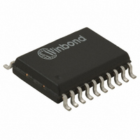
IC VOICEBAND CODEC 5V 1CH 20SOP
Manufacturer
Nuvoton Technology Corporation of America
Type
PCMr
Specifications of W681512SG TR
Data Interface
PCM Audio Interface
Resolution (bits)
8 b
Number Of Adcs / Dacs
1 / 1
Sigma Delta
No
Voltage - Supply, Analog
4.5 V ~ 5.5 V
Voltage - Supply, Digital
4.5 V ~ 5.5 V
Operating Temperature
-40°C ~ 85°C
Mounting Type
Surface Mount
Package / Case
20-SOP
Single Supply Voltage (typ)
5V
Single Supply Voltage (min)
4.5V
Single Supply Voltage (max)
5.5V
Lead Free Status / RoHS Status
Lead free / RoHS Compliant
For Use With
W681513DK - KIT DEVELOPMENT FOR W681513W681512DK - KIT DEVELOPMENT FOR W681512W681511DK - KIT DEVELOPMENT FOR W681511W681512ES - EVALUATION SYSTEM FOR W681512
Lead Free Status / RoHS Status
Compliant, Lead free / RoHS Compliant
Other names
W681512SG T&R
W681512SG T&R
W681512SG T&R


4. TABLE OF CONTENTS
1. GENERAL DESCRIPTION.................................................................................................................. 2
2. FEATURES ......................................................................................................................................... 2
3. BLOCK DIAGRAM .............................................................................................................................. 3
4. TABLE OF CONTENTS ...................................................................................................................... 4
5. PIN CONFIGURATION ....................................................................................................................... 6
6. PIN DESCRIPTION ............................................................................................................................. 7
7. FUNCTIONAL DESCRIPTION............................................................................................................ 8
8. TIMING DIAGRAMS.......................................................................................................................... 13
9. ABSOLUTE MAXIMUM RATINGS.................................................................................................... 20
10. ELECTRICAL CHARACTERISTICS ............................................................................................... 21
11. TYPICAL APPLICATION CIRCUIT ................................................................................................. 29
12. PACKAGE SPECIFICATION .......................................................................................................... 31
7.1. Transmit Path ................................................................................................................................ 8
7.2. Receive Path ................................................................................................................................. 9
7.3. Power Management..................................................................................................................... 10
7.4. PCM Interface .............................................................................................................................. 10
9.1. Absolute Maximum Ratings ......................................................................................................... 20
9.2. Operating Conditions ................................................................................................................... 20
10.1. General Parameters .................................................................................................................. 21
10.2. Analog Signal Level and Gain Parameters ...............................................................................22
10.3. Analog Distortion and Noise Parameters ..................................................................................23
10.4. Analog Input and Output Amplifier Parameters.........................................................................24
10.5. Digital I/O ................................................................................................................................... 26
12.1. 20L SOG (SOP)-300mil ............................................................................................................. 31
7.3.1. Analog and Digital Supply ..................................................................................................... 10
7.3.2. Analog Ground Reference Voltage Output ...........................................................................10
7.4.1. Long Frame Sync.................................................................................................................. 10
7.4.2. Short Frame Sync ................................................................................................................. 11
7.4.3. General Circuit Interface (GCI) ............................................................................................. 11
7.4.4. Interchip Digital Link (IDL)..................................................................................................... 12
7.4.5. System Timing ...................................................................................................................... 12
10.5.1. μ-Law Encode Decode Characteristics...............................................................................26
10.5.2. A-Law Encode Decode Characteristics ..............................................................................27
10.5.3. PCM Codes for Zero and Full Scale ...................................................................................28
10.5.4. PCM Codes for 0dBm0 Output ...........................................................................................28
- 4 -
W681512
Related parts for W681512SG TR
Image
Part Number
Description
Manufacturer
Datasheet
Request
R

Part Number:
Description:
IC VOICEBAND CODEC 5V 1CH 20SOP
Manufacturer:
Nuvoton Technology Corporation of America
Datasheet:
Part Number:
Description:
Manufacturer:
Nuvoton Technology Corporation of America
Datasheet:
Part Number:
Description:
Manufacturer:
Nuvoton Technology Corporation of America
Datasheet:
Part Number:
Description:
Manufacturer:
Nuvoton Technology Corporation of America
Datasheet:
Part Number:
Description:
Manufacturer:
Nuvoton Technology Corporation of America
Datasheet:
Part Number:
Description:
Manufacturer:
Nuvoton Technology Corporation of America
Datasheet:
Part Number:
Description:
Manufacturer:
Nuvoton Technology Corporation of America
Datasheet: