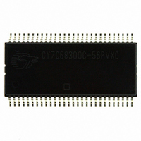
CY7C68300C-56PVXC Cypress Semiconductor Corp, CY7C68300C-56PVXC Datasheet - Page 11

CY7C68300C-56PVXC
Manufacturer Part Number
CY7C68300C-56PVXC
Description
IC USB 2.0 BRIDGE AT2LP 56-SSOP
Manufacturer
Cypress Semiconductor Corp
Series
CY7Cr
Type
USB to ATA/ATAPI Bridger
Datasheets
1.CY7C68300C-56PVXC.pdf
(42 pages)
2.CY7C68320C-100AXA.pdf
(44 pages)
3.CY7C68300C-56PVXC.pdf
(42 pages)
Specifications of CY7C68300C-56PVXC
Package / Case
56-SSOP
Controller Type
USB 2.0 Controller
Interface
I²C
Voltage - Supply
3.15 V ~ 3.45 V
Current - Supply
50mA
Operating Temperature
0°C ~ 70°C
Mounting Type
Surface Mount
Maximum Operating Temperature
+ 70 C
Minimum Operating Temperature
0 C
Mounting Style
SMD/SMT
Number Of Bits
48
Operating Temperature Range
0 C to + 70 C
Supply Current
10 mA
Operating Supply Voltage
3.3 V
Controller Family/series
(8051) USB
Core Size
8 Bit
No. Of I/o's
6
Embedded Interface Type
I2C, USB
Digital Ic Case Style
SSOP
Supply Voltage Range
3V To 3.6V
Rohs Compliant
Yes
Operating Temperature (min)
0C
Operating Temperature Classification
Commercial
Operating Temperature (max)
70C
Package Type
SSOP
Rad Hardened
No
Lead Free Status / RoHS Status
Lead free / RoHS Compliant
For Use With
CY4615B - KIT USB TO ATA REFERENCE DESIGN
Lead Free Status / Rohs Status
Lead free / RoHS Compliant
Other names
428-2266-5
CY7C68300C-56PVXC
CY7C68300C-56PVXC
Available stocks
Company
Part Number
Manufacturer
Quantity
Price
Company:
Part Number:
CY7C68300C-56PVXC
Manufacturer:
HITACHI
Quantity:
2 000
Company:
Part Number:
CY7C68300C-56PVXC
Manufacturer:
CY
Quantity:
8
Part Number:
CY7C68300C-56PVXC
Manufacturer:
CYPRESS/赛普拉斯
Quantity:
20 000
Table 1. AT2LP Pin Descriptions
Note: (Italic pin names denote pin functionality during CY7C68300A compatibility mode)
Document 001-05809 Rev. *B
TQFP
70
100
63
64
65
66
67
68
69
71
72
73
74
75
76
77
78
79
80
81
82
83
84
85
86
87
88
89
90
91
92
93
[3]
QFN
36
36
13
54
N/A
N/A
N/A
N/A
N/A
N/A
56
32
33
34
35
37
38
39
40
41
42
43
44
45
46
47
48
[3]
[3]
[3]
[3]
SSOP
N/A
N/A
N/A
N/A
N/A
N/A
N/A
56
39
40
41
42
43
44
45
46
47
48
49
50
51
52
53
54
55
(VBUS_PWR_VALID)
VBUS_ATA_ENABLE
DRVPWRVLD
Pin Name
ARESET#
(ATA_EN)
RESET#
INTRQ
GPIO0
GPIO1
GPIO2
GPIO3
GPIO4
GPIO5
(DA2)
DD10
CS0#
CS1#
DD11
GND
GND
GND
DD8
DD9
V
DA0
DA1
DA2
V
V
NC
NC
NC
CC
CC
CC
O/Z
O/Z
O/Z
O/Z
O/Z
O/Z
PWR
PWR
PWR
Type
GND
GND
I/O
I/O
I/O
I/O
I/O
Pin
NC
NC
NC
I
[1]
I
I
I
[1]
[1]
[1]
[1]
[3]
[1]
[1]
[1]
[1]
[1]
[1]
Default State
Driven HIGH
Driven HIGH
Driven HIGH
Driven HIGH
Driven HIGH
at Startup
after 2 ms
after 2 ms
after 2 ms
after 2 ms
after 2 ms
delay
delay
delay
delay
delay
Input
Input
Input
Input
Hi-Z
Hi-Z
Hi-Z
Hi-Z
No connect.
Ground.
V
ATA interrupt request.
ATA address.
ATA address.
Device presence detect. (See
page 14). Configurable logical polarity is controlled by
EEPROM address 0x08. This pin must be pulled HIGH
if functionality is not utilized.
Alternate function. Input when the EEPROM configu-
ration byte 8 has bit 7 set to one. The input value is
reported through EP1IN (byte 0, bit 0).
ATA chip select.
ATA chip select.
ATA address.
ATA reset.
Ground.
No connect.
Chip reset (See
V
VBUS detection (See
page 14).
ATA data bit 8.
ATA data bit 9.
ATA data bit 10.
ATA data bit 11.
Ground.
V
No connect.
General purpose I/O pins (See
page 14). The GPIO pins must be tied to GND if
functionality is not used.
CC
CC
CC
. Connect to 3.3V power source.
. Connect to 3.3V power source.
. Connect to 3.3V power source.
(continued)
CY7C68300C, CY7C68301C
CY7C68320C, CY7C68321C
“RESET#”
Pin Description
“VBUS_ATA_ENABLE”
on page 15).
“DRVPWRVLD”
“GPIO Pins”
Page 11 of 42
on
on
on
[+] Feedback


