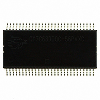
CY7C68300C-56PVXC Cypress Semiconductor Corp, CY7C68300C-56PVXC Datasheet - Page 20

CY7C68300C-56PVXC
Manufacturer Part Number
CY7C68300C-56PVXC
Description
IC USB 2.0 BRIDGE AT2LP 56-SSOP
Manufacturer
Cypress Semiconductor Corp
Series
CY7Cr
Type
USB to ATA/ATAPI Bridger
Datasheets
1.CY7C68300C-56PVXC.pdf
(42 pages)
2.CY7C68320C-100AXA.pdf
(44 pages)
3.CY7C68300C-56PVXC.pdf
(42 pages)
Specifications of CY7C68300C-56PVXC
Package / Case
56-SSOP
Controller Type
USB 2.0 Controller
Interface
I²C
Voltage - Supply
3.15 V ~ 3.45 V
Current - Supply
50mA
Operating Temperature
0°C ~ 70°C
Mounting Type
Surface Mount
Maximum Operating Temperature
+ 70 C
Minimum Operating Temperature
0 C
Mounting Style
SMD/SMT
Number Of Bits
48
Operating Temperature Range
0 C to + 70 C
Supply Current
10 mA
Operating Supply Voltage
3.3 V
Controller Family/series
(8051) USB
Core Size
8 Bit
No. Of I/o's
6
Embedded Interface Type
I2C, USB
Digital Ic Case Style
SSOP
Supply Voltage Range
3V To 3.6V
Rohs Compliant
Yes
Operating Temperature (min)
0C
Operating Temperature Classification
Commercial
Operating Temperature (max)
70C
Package Type
SSOP
Rad Hardened
No
Lead Free Status / RoHS Status
Lead free / RoHS Compliant
For Use With
CY4615B - KIT USB TO ATA REFERENCE DESIGN
Lead Free Status / Rohs Status
Lead free / RoHS Compliant
Other names
428-2266-5
CY7C68300C-56PVXC
CY7C68300C-56PVXC
Available stocks
Company
Part Number
Manufacturer
Quantity
Price
Company:
Part Number:
CY7C68300C-56PVXC
Manufacturer:
HITACHI
Quantity:
2 000
Company:
Part Number:
CY7C68300C-56PVXC
Manufacturer:
CY
Quantity:
8
Part Number:
CY7C68300C-56PVXC
Manufacturer:
CYPRESS/赛普拉斯
Quantity:
20 000
Table 8. Example CfgCB
MfgCB
The mfg_load and mfg_read vendor-specific commands are
passed down through the bulk pipe in the CBWCB portion of the
CBW. The format of this MfgCB is shown as follows. Byte0 is a
vendor-specific command designator whose value is config-
urable and set in the AT2LP configuration data. Byte 1 must be
0x27 to identify a MfgCB. Bytes 2 through 15 are reserved and
must be set to zero.
The data transfer length is determined by the CBW Data Transfer
Length specified in bytes 8 through 11 (dCBWDataTransfer-
Length) of the CBW. The type and direction of the command is
determined by the direction bit specified in byte 12, bit 7
(bmCBWFlags) of the CBW.
Table 9. Example MfgCB
Mfg_load
During a Mfg_load, the AT2LP enters into Manufacturing Test
Mode. Manufacturing Test Mode is provided as a means to
implement board or system level interconnect tests. During
Manufacturing Test Mode operation, all outputs not directly
associated with USB operation are controllable. Normal control
of the output pins are disabled. Control of the select AT2LP I/O
pins and their tri-state controls are mapped to the ATAPI data
packet associated with this request. (See
nation of the required Mfg_load data format.) Any data length can
be specified, but only bytes 0 through 3 are mapped to pins, so
a length of 4 bytes is recommended. To exit Manufacturing Test
Mode, a hard reset (toggle RESET#) is required.
Document 001-05809 Rev. *B
Offset
Offset
0
1
2
3
4
5
6–15
2–15 2–15 Reserved (must be zero) 0 0 0 0 0 0 0 0
0
1
0 bVSCBSignature
1 bVSCBSubCommand
bVSCBSignature (set in configuration bytes)
bVSCBSubCommand (must be 0x26)
Reserved (must be set to zero)
Data Source (must be set to 0x02)
Start Address (LSB) (must be set to zero)
Start Address (MSB) (must be set to zero)
Reserved (must be set to zero)
MfgCB Byte Description
(set in configuration bytes)
(hardcoded 0x27)
CfgCB Byte Descriptions
7 6 5 4 3 2 1 0
0 0 1 0 0 1 0 0
0 0 1 0 0 1 1 1
Table 10
Bits
for an expla-
Mfg_read
This USB request returns a ’snapshot’ of select AT2LP input
pins. AT2LP input pins not directly associated with USB
operation can be sampled at any time during Manufacturing Test
Mode operation. See
Mfg_read data format. Any data length can be specified, but only
bytes 0 through 3 contain usable information, so a length of 4
bytes is recommended.
Table 10. Mfg_read and Mfg_load Data Format
Byte
0
1
2
3
7
0
0
0
0
0
0
0
Bits
5:4
2:1
7:0
7:0
6
0
0
0
0
0
0
0
7
6
3
0
7
6
5
4
3
2
1
0
CY7C68300C, CY7C68301C
CY7C68320C, CY7C68321C
Read/Load
5
1
1
0
0
0
0
0
R/L
R/L
R/L
R/L
R/L
R/L
R/L
R/L
R/L
R
R
R
R
R
R
L
Table 10
4
0
0
0
0
0
0
0
Bits
ARESET#
DA2
CS#[1:0]
DRVPWRVLD
DA[1:0]
INTRQ
DD[15:0] High-Z Status
0 = Hi-Z all DD pins
1 = Drive DD pins
MFG_SEL
0 = Mass Storage Mode
1 = Manufacturing Mode
VBUS_ATA_ENABLE
DMARQ
IORDY
DMACK#
DIOR#
DIOW#
DD[7:0]
DD[15:8]
3
0
0
0
0
0
0
0
for an explanation of the
2
1
1
0
0
0
0
0
Function
1
0
1
0
1
0
0
0
Page 20 of 42
0
0
0
0
0
0
0
0
[+] Feedback


