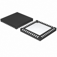
SI3452C-B01-GM Silicon Laboratories Inc, SI3452C-B01-GM Datasheet - Page 26

SI3452C-B01-GM
Manufacturer Part Number
SI3452C-B01-GM
Description
IC POE CONTROLLER MIDSPAN 40QFN
Manufacturer
Silicon Laboratories Inc
Datasheet
1.SI3452B-B01-GM.pdf
(36 pages)
Specifications of SI3452C-B01-GM
Package / Case
40-QFN
Controller Type
Power over Ethernet Controller (POE)
Interface
I²C
Voltage - Supply
3 V ~ 3.6 V
Current - Supply
14mA
Operating Temperature
-40°C ~ 85°C
Mounting Type
Surface Mount
Maximum Power Dissipation
1.2 W
Minimum Operating Temperature
- 40 C
Mounting Style
SMD/SMT
Product
Ethernet Controllers
Standard Supported
IEEE 802.3at, IEEE 802.3af
Supply Voltage (max)
3.6 V
Supply Voltage (min)
3 V
Supply Current (max)
14 mA
Maximum Operating Temperature
+ 85 C
Operating Temperature (max)
85C
Operating Temperature (min)
-40C
Pin Count
40
Mounting
Surface Mount
Package Type
QFN EP
Case Length
6mm
Case Height
0.83mm
Screening Level
Industrial
Lead Free Status / RoHS Status
Lead free / RoHS Compliant
Lead Free Status / RoHS Status
Lead free / RoHS Compliant, Lead free / RoHS Compliant
Other names
336-1834-5
Available stocks
Company
Part Number
Manufacturer
Quantity
Price
Company:
Part Number:
SI3452C-B01-GM
Manufacturer:
HITTITE
Quantity:
1 145
Si3452
7. PCB Layout Guidelines
Following are some PCB layout considerations. See also "12.1. Evaluation Kits and Reference Designs" on page
33 for reference design information. Please visit the Silicon Labs technical support web page at
www.silabs.com/support/pages/contacttechnicalsupport.aspx
and register to request support for your design,
particularly if you are not closely following the recommended reference design.
Due to the high current of up to 800 mA per port, the following board layout guidelines apply. In addition, contact
Silicon Laboratories for access to complete PSE reference design databases including recommended layouts.
The VEE1, VEE2, VEE3, and VEE4 pins can carry up to 800 mA and are connected to a V
bus. The V
bus for
EE
EE
a 24 port PCB layout can thus carry as much as 20 A current. With 2 oz. copper on an outer layer, a bus of 0.4
inches is needed. For an inner layer, this increases to a 1 inch wide bus. Use of large or multiple vias is required for
properly supporting the 800 mA per channel operating current. The VEE pin does not carry high current and can be
connected directly to the bus as well. The best practice is to devote an entire inner layer for V
power routing.
EE
Similarly, GND1/2 and GND3/4 pins can carry up to 1.6 A per pin, and the GND return bus should be at least as
wide as the V
bus described above. The best practice is to devote an entire inner layer for ground power routing.
EE
The ground power plane does not generally have a high frequency content (other than external faults); so, it is
generally acceptable to use the ground power plane as a ground signal plane and tie AGND and GND12, GND34
to this plane as well.
The VOUTn pins carry up to 800 mA dc and up to 5 A in faults; so, a 20 mil trace with wide or multiple vias is also
recommended. The VDETn pins also carry fault current; so, this pin connection to VOUTn needs to use 20 mil
traces and wide or multiple vias where needed.
The VDD currents are not large; so, it is acceptable to route the VDD nodes on one of the outer layers.
If care is taken to avoid disruption of the high current paths, VDD can be globally routed on one of the power planes
and then locally routed on an inner or outer layer.
To avoid coupling between surge events and logic signals, it is recommended that VOUTn traces be routed on the
2
side opposite the I
C interface pins.
The thermal pad of the Si3452 is connected to VEE. At full IEEE 802.3at current of 600 mA on each port, the
dissipation of the Si3452 is up to 1.2 W; so, multiple vias are required to conduct the heat from the thermal pad to
the VEE plane. As many as 36 small vias provide the best thermal conduction.
26
Rev. 1.2


