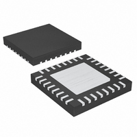
MAX3421EETJ+T Maxim Integrated Products, MAX3421EETJ+T Datasheet - Page 5

MAX3421EETJ+T
Manufacturer Part Number
MAX3421EETJ+T
Description
IC USB PERIPH/HOST CNTRL 32TQFN
Manufacturer
Maxim Integrated Products
Datasheet
1.MAX3421EETJ.pdf
(32 pages)
Specifications of MAX3421EETJ+T
Controller Type
USB Peripheral Controller
Interface
USB/Serial
Voltage - Supply
3 V ~ 3.6 V
Current - Supply
15mA
Operating Temperature
-40°C ~ 85°C
Mounting Type
Surface Mount
Package / Case
32-TQFN Exposed Pad
For Use With
MAX3421EVKIT-1+ - EVAL KIT FOR MAX3421E
Lead Free Status / RoHS Status
Lead free / RoHS Compliant
3, 19
PIN
10
11
12
13
14
15
16
17
18
20
1
2
4
5
6
7
8
9
GPOUT0
GPOUT1
GPOUT2
GPOUT3
GPOUT4
GPOUT5
GPOUT6
GPOUT7
NAME
GPIN7
SCLK
MISO
MOSI
GND
GPX
RES
INT
V
SS
D-
L
_______________________________________________________________________________________
OUTPUT
Input or
INPUT/
Output
Output
Output
Output
Output
Output
Input/
Input/
Input
Input
Input
Input
Input
Input
General-Purpose Input. GPIN7–GPIN0 are connected to V
GPIN7–GPIN0 logic levels are referenced to the voltage on V
Level-Translator Voltage Input. Connect V
supply. Bypass V
Ground
General-Purpose Push-Pull Outputs. GPOUT7–GPOUT0 logic levels are referenced to the
voltage on V
Device Reset. Drive RES low to clear all of the internal registers except for PINCTL (R17),
USBCTL (R15), and SPI logic. The logic level is referenced to the voltage on V
Device Reset section for a description of resets available on the MAX3421E.) Note: The
MAX3421E is internally reset if either V
under these conditions.
S P I S er i al - C l ock Inp ut. An exter nal S P I m aster sup p l i es S C LK w i th fr eq uenci es up to 26M H z. The
l og i c l evel i s r efer enced to the vol tag e on V
r i si ng ed g e of S C LK. D ata i s cl ocked out of the S P I sl ave i nter face on the fal l i ng ed g e of S C LK.
SPI Slave Select Input. The SS logic level is referenced to the voltage on V
high, the SPI slave interface is not selected, the MISO pin is high impedance, and SCLK
transitions are ignored. An SPI transfer begins with a high-to-low SS transition and ends with a
low-to-high SS transition.
SPI Serial-Data Output (Master-In Slave-Out). MISO is a push-pull output. MISO is tri-stated in
half-duplex mode or when SS = 1. The MISO logic level is referenced to the voltage on V
SPI Serial-Data Input (Master-Out Slave-In). The logic level on MOSI is referenced to the
voltage on V
(See Figure 15.)
G ener al - P ur p ose M ul ti p l exed P ush- P ul l O utp ut. The i nter nal M AX 3421E si g nal that ap p ear s on
G P X i s p r og r am m ab l e b y w r i ti ng to the G P X B and G P X A b i ts of the P IN C TL ( R17) r eg i ster and the
S E P IRQ b i t of the M O D E ( R27) r eg i ster . GP X i nd i cates one of fi ve si g nal s ( see the G P X secti on) .
Interrupt Output. In edge mode, the logic level on INT is referenced to the voltage on V
a push-pull output with programmable polarity. In level mode, INT is open-drain and active low.
Set the IE bit in the CPUCTL (R16) register to enable INT.
USB D- Signal. Connect D- to a USB connector through a 33Ω ±1% series resistor. A
switchable 15kΩ D- pulldown resistor is internal to the device.
USB Peripheral/Host Controller
L
L
.
. MOSI can also be configured as a bidirectional MOSI/MISO input and output.
L
to ground with a 0.1µF capacitor as close to V
C C
L
L
or V
FUNCTION
. D ata i s cl ocked i nto the S P I sl ave i nter face on the
to the system’s 1.4V to 3.6V logic-level power
L
with SPI Interface
is not present. The register file is not accessible
L
with internal pullup resistors.
L
.
L
as possible.
Pin Description
L
. When SS is driven
L
. (See the
L
and is
L
.
5


