DS2143 Maxim Integrated Products, DS2143 Datasheet
DS2143
Specifications of DS2143
Available stocks


Related parts for DS2143

DS2143 Summary of contents
Page 1
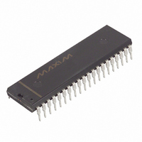
... Available in 40-pin DIP and 44-pin PLCC (DS2143Q) DESCRIPTION The DS2143 is a comprehensive, software-driven E1 framer meant to act as a slave or coprocessor to a microcontroller or microprocessor. Quick access via the parallel control port allows a single micro to handle many E1 lines. The DS2143 is very flexible and can be configured into numerous orientations via software ...
Page 2
... This information will be used by the rest of the receive side circuitry. The DS2143 is an “off-line” framer, which means that all of the E1 serial stream that goes into the device will come out of it unchanged. Once the E1 data has been framed to, the signaling data can be extracted. ...
Page 3
... Loss of transmit clock detection HDB3 coder/decoder Full transmit transparency Large error counters Individual bit-by-bit Sa data link support circuitry Programmable output clocks Frame sync generation Local loopback capability Automatic CRC4 E-bit support Loss of receive clock detection G.802 mapping support DS2143 BLOCK DIAGRAM DS2143/DS2143Q ...
Page 4
... Tie together to receive NRZ data and disable BPV monitoring circuitry. System Clock. 1.544 MHz or 2.048 MHz clock. Only used when the elastic store function is enabled via the RCR2.1. Should be tied low in applications that do not use the elastic store DS2143/DS2143Q ) pins. If BTS=1, then these pins W ...
Page 5
... TCLK to insert Sa bits. See Section 13 for timing details. Transmit Sync. A pulse at this pin will establish either frame or CAS multiframe boundaries for the DS2143. Via TCR1.1, the DS2143 can be programmed to output either a frame or multiframe pulse at this pin. See Section 13 for timing details. Positive Supply. 5.0 volts ...
Page 6
... DS2143 REGISTER MAP ADDRESS HEX R 00000000 00 R Bipolar Violation Count Register 1. 00000001 01 R Bipolar Violation Count Register 2. 00000010 02 R CRC4 Count Register 1. 00000011 03 R CRC4 Count Register 2. 00000100 04 R E-Bit Count Register 1. 00000101 05 R E-Bit Count Register 2. 00000110 06 R/W Status Register 1 ...
Page 7
... Signaling Register 14. REGISTER ADDRESS NAME 00111110 00111111 01000000 01000001 01000010 01000011 01000100 01000101 01000110 01000111 01001000 01001001 01001010 01001011 01001100 DS2143/DS2143Q HEX R/W REGISTER NAME 3E R Receive Signaling Register 15 Receive Signaling Register 16. 40 R/W Transmit Signaling Register 1. 41 R/W Transmit Signaling Register 2 ...
Page 8
... Receive Control Registers (RCR1 and RCR2), two Transmit Control Registers (TCR1 and TCR2), and a Common Control Register (CCR). Each of the five registers is described in this section. The Test Register at address 15 hex is used by the factory in testing the DS2143. On power-up, the Test Register should be set to 00 hex in order for the DS2143 to operate properly. ...
Page 9
... FAS received in error 3 consecutive times 1 = resync if FAS or bit 2 of non-FAS is received in error 3 consecutive times Sync Enable auto resync enabled 1 = auto resync disabled Resync. When toggled from low to high, a resync is initiated. Must be cleared and set again for a subsequent resync DS2143/DS2143Q (LSB) SYNCE RESYNC ...
Page 10
... Sa4 bit. SYSCLK Mode Select SYSCLK is 1.544 MHz SYSCLK is 2.048 MHz. Elastic Store Enable elastic store is bypassed elastic store is enabled. Not Assigned. Should be set to 0 when written to DS2143/DS2143Q ITU SPEC. G.706 4.1.1 4.1.2 G.706 4.2 4.3.2 G.732 5 ...
Page 11
... Transmit Signaling All 1s normal operation force timeslot 16 in every frame to all 1s. TSYNC Mode Select frame mode (see the timing in Section 13 CAS and CRC4 multiframe mode (see the timing in Section 13). TSYNC I/O Select TSYNC is an input TSYNC is an output DS2143/DS2143Q (LSB) TSM TSIO ...
Page 12
... Sa4 bit. Not Assigned. Should be set to 0 when written to. Automatic E-Bit Enable E-bits not automatically set in the transmit direction E-bits automatically set in the transmit direction. Function of Pin 34 Receive Loss of Sync (RLOS Loss of Transmit Clock (LOTC DS2143/DS2143Q (LSB) - AEBE P34F ...
Page 13
... CCR.0 LOCAL LOOPBACK When CCR.7 is set the DS2143 will enter a Local LoopBack (LLB) mode. This loopback is useful in testing and debugging applications. In LLB, the DS2143 will loop data from the transmit side back to the receive side. This loopback is synonymous with replacing the RCLK input with the TCLK signal, and the RPOS/RNEG inputs with the TPOS/TNEG outputs. When LLB is enabled, the following will occur: 1. data at RPOS and RNEG will be ignored ...
Page 14
... STATUS AND INFORMATION REGISTERS There is a set of four registers that contain information on the current real time status of the DS2143: Status Register 1 (SR1), Status Register 2 (SR2), Receive Information Register (RIR), and Synchronizer Status Register (SSR). When a particular event has occurred (or is occurring), the appropriate bit in one of these three registers will be set ...
Page 15
... Not Assigned. Could be any value when read. FAS Resync Criteria Met. Set when three consecutive FAS words are received in error. CAS Resync Criteria Met. Set when two consecutive CAS MF alignment words are received in error DS2143/DS2143Q (LSB) - FASRC CASRC ...
Page 16
... CRC4 mode (CCR.0=0). This counter is useful for determining the amount of time the DS2143 has been searching for synchronization at the CRC4 level. Annex B of CCITT G.706 suggests that if synchronization at the CRC4 level cannot be obtained within 400 ms, then the search should be abandoned and proper action taken ...
Page 17
... RPOS and RNEG. Receive Remote Alarm. Set when a remote alarm is received at RPOS and RNEG. Receive Carrier Loss. Set when 255 consecutive 0s have been detected at RPOS and RNEG. Receive Loss of Sync. Set when the device is not synchronized to the receive E1 stream DS2143/DS2143Q (LSB) RCL RLOS ...
Page 18
... MFs more than two 0s in two frames (512 bits) bit 3 of non-align frame set to 0 for three consecutive occasions in 255 bit times, at least 32 1s are received DS2143/DS2143Q ITU SPEC. G.732 4.2 G.732 5.2 O.162 2.1.5 O ...
Page 19
... Will force pin 34 high if enabled via TCR2.0. Based on RCLK. Receive CRC4 Multiframe. Set on CRC4 multiframe boundaries; will continue to be set every arbitrary boundary if CRC4 is disabled. Loss of Receive Clock. Set when the RCLK pin has not transitioned for at least ±1 s DS2143/DS2143Q (LSB) RCMF LORC ...
Page 20
... Elastic Store Slip Occurrence interrupt masked interrupt enabled. Receive Unframed All 1s interrupt masked interrupt enabled. Receive Remote Alarm interrupt masked interrupt enabled. Receive Carrier Loss interrupt masked interrupt enabled. Receive Loss of Sync interrupt masked interrupt enabled DS2143/DS2143Q (LSB) RCL RLOS ...
Page 21
... IMR2.0 5.0 ERROR COUNT REGISTERS There are a set of three counters in the DS2143 that record bipolar violations, errors in the CRC4 SMF code words, and E-bits as reported by the far end. Each of these three counters are automatically updated on 1-second boundaries as determined by the 1-second timer in Status Register 2 (SR2.4). Hence, these registers contain performance data from the previous second ...
Page 22
... MSB of the bipolar violation count. LSB of the bipolar violation count. CRC4 CRC3 CRC2 CRC12 CRC11 CRC10 NAME AND DESCRIPTION MSB of the CRC4 error count. LSB of the CRC4 error count DS2143/DS2143Q (LSB) BV1 BV0 BPVCR2 BV9 BV8 BPVCR1 (LSB) CRC1 CRC0 CRCCR2 ...
Page 23
... TLINK pin. If the user wishes to pass the Sa bits through the DS2143 without them being altered, then the device should be set up to source all 5 Sa bits via the TLINK pin and the TLINK pin should be tied to the TSER pin. Please see the timing diagrams and the transmit data flow diagram in Section 13 for examples ...
Page 24
... A(28) B(28) D(14) A(29) B(29) D(15) A(30) B(30) NAME AND DESCRIPTION Spare Bits. Remote Alarm Bit (integrated and reported in SR1.6). Signaling Bit A for Channel 1. Signaling Bit D for Channel 30 DS2143/DS2143Q (LSB RS1 (30) C(16) D(16) RS2 (31) C(17) D(17) RS3 (32) C(18) D(18) RS4 (33) ...
Page 25
... TRANSMIT IDLE REGISTERS There is a set of five registers in the DS2143 that can be used to custom tailor the data that transmitted onto the E1 line channel by channel basis. Each of the 32 E1 channels can be forced to have a user defined idle code inserted into them. ...
Page 26
... Transmit Idle Registers not insert the Idle Code into this channel insert the Idle Code into this channel. TIDR4 TIDR3 TIDR2 NAME AND DESCRIPTION MSB of the Idle Code. LSB of the Idle Code DS2143/DS2143Q (LSB) CH2 CH1 TIR1 (26) CH10 CH9 TIR2 (27) CH18 CH17 ...
Page 27
... TCBR1.0 10.0 ELASTIC STORE OPERATION The DS2143 has an onboard two-frame (512 bits) elastic store. This elastic store can be enabled via RCR2.1. If the elastic store is enabled (RCR2.1=1), then the user must provide either a 1.544 MHz (RCR2.2=0) or 2.048 MHz (RCR2.2=1) clock at the SYSCLK pin. If the elastic store is enabled, then the user has the option of either providing a frame sync at the RFSYNC pin (RCR1 ...
Page 28
... TAF and TNAF registers. It has 250 s to update the data or else the old data will be retransmitted. Data in the Si bit position will be overwritten if either the DS2143 is programmed: (1) to source the Si bits from the TSER pin, (2) in the CRC4 mode, or (3) have automatic E-bit insertion enabled. Data in the Sa bit position will be overwritten if any of the TCR2 ...
Page 29
... Additional Bit NAME AND DESCRIPTION International Bit. Frame Alignment Signal Bit. Frame Alignment Signal Bit. Frame Alignment Signal Bit. Frame Alignment Signal Bit. Frame Alignment Signal Bit. Frame Alignment Signal Bit. Frame Alignment Signal Bit DS2143/DS2143Q (LSB) Sa6 Sa7 Sa8 (LSB ...
Page 30
... TNAF.0 12.0 LINE INTERFACE CONTROL FUNCTION The DS2143 can control line interface units that contain serial ports. When Control Register Bytes (CRB1, CRB2) are written to, the DS2143 will automatically write this data serially (LSB first) into the line interface by creating a chip select, serial clock and serial data via the LI_ pins respectively ...
Page 31
... Data from the E1 channels 13, 17, 21, 25, and 29 is dropped (channel 2 from the E1 link is mapped to channel 1 of the T1 link, etc.) and the F-bit position is added (forced to 1). 2. RSYNC is in the output mode (RCR1.5=0). 3. RSYNC is in the input mode (RCR1.5=1). 4. RCHBLK is programmed to block channel 24 DS2143/DS2143Q ...
Page 32
... NOTES: 1. There RCLK delay from RPOS, RNEG to RSER. 2. RCHBLK is programmed to block channel 2. 3. RLINK is programmed to output the Sa4 bits. 4. RLINK is programmed to output the Sa4 and Sa8 bits. 5. RLINK is programmed to output the Sa5 and Sa7 bits. 6. Shown is a non-align frame boundary DS2143/DS2143Q ...
Page 33
... There TCLK delay from TSER to TPOS, and TNEG. 2. TSYNC is in the input mode (TCR1.0=0). 3. TSYNC is in the output mode (TCR1.0=1). 4. TCHBLK is programmed to block channel 2. 5. TLINK is programmed to source the Sa4 bits. 6. TLINK is programmed to source the Sa7 and Sa8 bits. 7. Shown is a non-align frame boundary DS2143/DS2143Q ...
Page 34
... This diagram assumes both the CAS MF and the CRC4 begin with the align frame. LINE INTERFACE CONTROL TIMING NOTES write to CRB1 will cause the DS2143 to output this sequence write to CRB2 will cause the DS2143 to output this sequence. 3. Timing numbers are based on RCLK=2.048 MHz with 50% duty cycle. ...
Page 35
... DS2143 SYNCHRONIZATION FLOWCHART DS2143/DS2143Q ...
Page 36
... DS2143 TRANSMIT DATA FLOW DS2143/DS2143Q ...
Page 37
... INT1 INT2 -1.0V to +7. - +125 C 260 C for 10 seconds SYMBOL MIN TYP 4.5 DD SYMBOL MIN TYP OUT ( SYMBOL MIN TYP - 5.5V DS2143/DS2143Q ( MAX UNITS NOTES V +0 +0.8 V 5.5 V MAX UNITS NOTES 10%) DD MAX UNITS NOTES 10 mA +1 ...
Page 38
... Output Data Delay Time from DS or Data Setup Time ( SYMBOL MIN t 250 CYC PW 150 EL PW 100 RWH t 50 RWS DHR t 0 DHW t 20 ASL t 10 AHL t 25 ASD PW 40 ASH ASED DDR t 80 DSW DS2143/DS2143Q = 5V + 10%) DD TYP MAX UNITS NOTES 100 ns ns ...
Page 39
... INTEL WRITE AC TIMING INTEL READ AC TIMING MOTOROLA AC TIMING DS2143/DS2143Q ...
Page 40
... RCLK and SYSCLK Pulse Width RPOS, RNEG, RSYNC Setup to RCLK Falling RPOS, RNEG, Hold from RCLK Falling RCLK Rise/Fall Times Data Delay RSYNC Pulse Width ( SYMBOL MIN TYP MAX UNITS t 488 SYMBOL MIN TYP MAX UNITS t 488 DS2143/DS2143Q = 5V 10%) DD NOTES =10%) DD NOTES ...
Page 41
... TRANSMIT SIDE AC TIMING NOTES: 1. TSYNC is in the output mode (TCR1.0=1). 2. TSYNC is in the input mode (TCR1.0=0 timing relationship between TSYNC and TLCLK/TLINK is implied DS2143/DS2143Q ...
Page 42
... RECEIVE SIDE AC TIMING NOTES: 1. RSYNC is in the output mode (RCR1.5=0). 2. RSYNC is in the input mode (RCR1.5=1 timing relationship between RSYNC and RLCLK/RLINK is implied DS2143/DS2143Q ...
Page 43
... DS2143 E1 CONTROLLER (600 MIL) 40-PIN DIP INCHES DIM MIN MAX A 2.040 2.070 B 0.530 0.560 C 0.145 0.155 D 0.600 0.625 E 0.015 0.040 F 0.120 0.140 G 0.090 0.110 H 0.625 0.675 J 0.008 0.012 K 0.015 0.022 DS2143/DS2143Q ...
Page 44
... DS2143 E1 CONTROLLER 44-PIN PLCC NOTE1: PIN 1 IDENTIFIER TO BE LOCATED IN ZONE INDICATED. INCHES DIM MIN MAX A 0.165 0.180 A1 0.090 0.120 A2 0.020 - B 0.026 0.033 B1 0.013 0.021 C 0.009 0.012 CH1 0.042 0.048 D 0.685 0.695 D1 0.650 0.656 D2 0.590 0.630 E 0.685 0.695 E1 0.650 0.656 E2 0.590 0.630 e1 0 ...