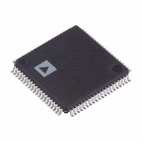
AD9852ASTZ Analog Devices Inc, AD9852ASTZ Datasheet - Page 32

AD9852ASTZ
Manufacturer Part Number
AD9852ASTZ
Description
IC DDS SYNTHESIZER CMOS 80-LQFP
Manufacturer
Analog Devices Inc
Datasheet
1.AD9852ASTZ.pdf
(52 pages)
Specifications of AD9852ASTZ
Resolution (bits)
12 b
Master Fclk
200MHz
Tuning Word Width (bits)
48 b
Voltage - Supply
3.14 V ~ 3.47 V
Operating Temperature
-40°C ~ 85°C
Mounting Type
Surface Mount
Package / Case
80-LQFP
Pll Type
Frequency Synthesis
Frequency
100MHz
Supply Current
660mA
Supply Voltage Range
3.135V To 3.465V
Digital Ic Case Style
LQFP
No. Of Pins
80
Operating Temperature Range
-40°C To +85°C
Lead Free Status / RoHS Status
Lead free / RoHS Compliant
For Use With
AD9852/PCBZ - BOARD EVAL FOR AD9852
Lead Free Status / RoHS Status
Lead free / RoHS Compliant, Lead free / RoHS Compliant
Available stocks
Company
Part Number
Manufacturer
Quantity
Price
Company:
Part Number:
AD9852ASTZ
Manufacturer:
ALTERA
Quantity:
210
Company:
Part Number:
AD9852ASTZ
Manufacturer:
Analog Devices Inc
Quantity:
135
Company:
Part Number:
AD9852ASTZ
Manufacturer:
ADI
Quantity:
260
Company:
Part Number:
AD9852ASTZ
Manufacturer:
Analog Devices Inc
Quantity:
10 000
Part Number:
AD9852ASTZ
Manufacturer:
ADI/亚德诺
Quantity:
20 000
AD9852
Table 9. Register Layout
Parallel
Address
(Hex)
00
01
02
03
04
05
06
07
08
09
0A
0B
0C
0D
0E
0F
10
11
12
13
14
15
16
17
18
19
1A
1B
1C
1D
1E
1F
20
21
22
23
24
25
26
27
1
The shaded sections comprise the control register.
Serial
Address
(Hex)
0
1
2
3
5
6
7
8
9
A
B
1
Bit 7
Phase Adjust Register 1 <13:8> (Bits 15, 14 don’t care)
Phase Adjust Register 1 <7:0>
Phase Adjust Register 2 <13:8> (Bits 15, 14 don’t care)
Phase Adjust Register 2 <7:0>
Frequency Tuning Word 1 <47:40>
Frequency Tuning Word 1 <39:32>
Frequency Tuning Word 1 <31:24>
Frequency Tuning Word 1 <23:16>
Frequency Tuning Word 1 <15:8>
Frequency Tuning Word 1 <7:0>
Frequency Tuning Word 2 <47:40>
Frequency Tuning Word 2 <39:32>
Frequency Tuning Word 2 <31:24>
Frequency Tuning Word 2 <23:16>
Frequency Tuning Word 2 <15:8>
Frequency Tuning Word 2 <7:0>
Delta frequency word <47:40>
Delta frequency word <39:32>
Delta frequency word <31:24>
Delta frequency word <23:16>
Delta frequency word <15:8>
Delta frequency word <7:0>
Update clock <31:24>
Update clock <23:16>
Update clock <15:8>
Update clock <7:0>
Ramp rate clock <19:16> (Bits 23, 22, 21, 20, don’t care)
Ramp rate clock <15:8>
Ramp rate clock <7:0>
Don’t care
CR [31]
Don’t care
CLR ACC1
Don’t care
Output shaped keying multiplier <11:8> (Bits 15, 14, 13, 12 don’t care)
Output shaped keying multiplier <7:0>
Don’t care
Don’t care
Output shaped keying ramp rate <7:0>
Control DAC <11:8> (Bits 15, 14, 13, 12 don’t care)
Control DAC <7:0> (Data is required to be in twos complement format)
Bit 6
Don’t care
PLL range
CLR ACC2
Bypass inv
sinc
Bit 5
Don’t
care
Bypass
PLL
Triangle
OSK EN
Rev. E | Page 32 of 52
AD9852 Register Layout
Bit 4
Comp
PD
Ref
Mult 4
Don’t
care
OSK INT
Bit 3
Reserved,
always
low
Ref
Mult 3
Mode 2
Don’t care
Bit 2
Phase 1
Phase 2
Frequency 1
Frequency 2
Control
DAC PD
Ref Mult 2
Mode 1
Don’t care
DAC PD
Ref
Mult 1
Mode 0
LSB first
Bit 1
Bit 0
DIG PD
Ref Mult 0
Int/Ext
update clock
SDO active
CR [0]
Default
Value
(Hex)
00
00
00
00
00
00
00
00
00
00
00
00
00
00
00
00
00
00
00
00
00
00
00
00
00
00
00
00
00
10
64
01
20
00
00
00
00
80
00
00


