ADM3222ARWZ Analog Devices Inc, ADM3222ARWZ Datasheet - Page 8
ADM3222ARWZ
Manufacturer Part Number
ADM3222ARWZ
Description
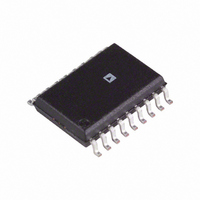
IC TXRX RS-232 3.3V W/SD 18-SOIC
Manufacturer
Analog Devices Inc
Type
Transceiverr
Datasheet
1.ADM3202ARUZ.pdf
(12 pages)
Specifications of ADM3222ARWZ
Number Of Drivers/receivers
2/2
Protocol
RS232
Voltage - Supply
3 V ~ 5.5 V
Mounting Type
Surface Mount
Package / Case
18-SOIC (7.5mm Width)
Device Type
Transceiver
Ic Interface Type
RS232
No. Of Drivers
2
Supply Voltage Range
3V To 5.5V
Driver Case Style
SOIC
No. Of Pins
18
Operating Temperature Range
-40°C To +85°C
Lead Free Status / RoHS Status
Lead free / RoHS Compliant
Available stocks
Company
Part Number
Manufacturer
Quantity
Price
Company:

Part Number:
ADM3222ARWZ
Manufacturer:
AD
Quantity:
2 197
Part Number:
ADM3222ARWZ
Manufacturer:
ADI/亚德诺
Quantity:
20 000
Company:
Part Number:
ADM3222ARWZ-REEL
Manufacturer:
SANYO
Quantity:
1 000
Part Number:
ADM3222ARWZ-REEL
Manufacturer:
ADI/亚德诺
Quantity:
20 000


ADM3202/ADM3222/ADM1385
GENERAL DESCRIPTION
The ADM3202/ADM3222/ADM1385 are RS-232 line drivers/
receivers. Step-up voltage converters coupled with level-shifting
transmitters and receivers allow RS-232 levels to be developed
while operating from a single 3.3 V supply.
CMOS technology is used to keep the power dissipation to an
absolute minimum, allowing maximum battery life in portable
applications.
The ADM3202/ADM3222/ADM1385 are modifications,
enhancements, and improvements of the AD230 to AD241
family and derivatives. They are essentially plug-in compatible
and do not have any materially different applications.
CIRCUIT DESCRIPTION
The internal circuitry consists of these main sections:
•
•
•
Charge Pump DC to DC Voltage Converter
The charge pump voltage converter consists of a 200 kHz
oscillator and a switching matrix. The converter generates a
stages by using a switched capacitor technique as illustrated in
Figure 18 and Figure 19. First, the 3.3 V input supply is doubled
to 6.6 V by using Capacitor C1 as the charge storage element.
The +6.6 V level is then inverted to generate −6.6 V using C2
as the storage element. C3 is shown connected between V+ and
V
Capacitors C3 and C4 are used to reduce the output ripple.
Their values are not critical and can be increased, if desired.
Capacitor C3 is shown connected between V+ and V
also acceptable to connect this capacitor between V+ and GND.
If desired, larger capacitors (up to 10 μF) can be used for
Capacitors C1 to C4.
±6.6 V supply from the input 3.3 V level. This is done in two
CC
OUTPUTS
INPUTS
but is equally effective if connected between V+ and GND.
A charge pump voltage converter
3.3 V logic to EIA-232 transmitters
EIA-232 to 5 V logic receivers
CMOS
CMOS
0.1µF
0.1µF
R1
R2
10V
10V
Figure 15. ADM3202 Typical Operating Circuit
T1
T2
OUT
OUT
IN
IN
+
+
GND
C1+
C1–
C2+
C2–
T1
+3.3V TO +6.6V
+6.6V TO –6.6V
ADM3202
INVERTER
DOUBLER
VOLTAGE
VOLTAGE
T2
*INTERNAL 5kΩ PULL-DOWN RESISTOR
ON EACH RS-232 INPUT
R1
R2
V
V+
CC
V–
+3.3V INPUT
+
+
T1
T2
R1
R2
C3
0.1µF
6.3V
C4
0.1µF
10V
OUT
OUT
IN
IN
EIA/TIA-232
OUTPUTS
EIA/TIA-232
INPUTS*
+
CC
C5
0.1µF
. It is
Rev. D | Page 8 of 12
OUTPUTS
OUTPUTS
DOUBLER
VOLTAGE
INPUTS
INPUTS
CMOS
CMOS
CMOS
CMOS
FROM
OSCILLATOR
GND
V
INTERNAL
0.1µF
0.1µF
CC
OSCILLATOR
R1
R2
0.1µF
0.1µF
GND
INTERNAL
R1
R2
10V
10V
10V
10V
T1
T2
V
OUT
OUT
Figure 16. ADM3222 Typical Operating Circuit
Figure 17. ADM1385 Typical Operating Circuit
T1
T2
OUT
OUT
+
IN
IN
+
+
IN
IN
Figure 18. Charge Pump Voltage Doubler
Figure 19. Charge Pump Voltage Inverter
DD
+
+
EN
S2
S1
GND
C1+
C1–
C2+
C2–
GND
C1+
C1–
C2+
C2–
S2
S1
T1
T1
+3.3V TO +6.6V
+6.6V TO –6.6V
+3.3V TO +6.6V
+6.6V TO –6.6V
INVERTER
C1
DOUBLER
T2
VOLTAGE
VOLTAGE
INVERTER
DOUBLER
T2
VOLTAGE
VOLTAGE
C2
*INTERNAL 5kΩ PULL-DOWN RESISTOR
ADM1385
ON EACH RS-232 INPUT
*INTERNAL 5kΩ PULL-DOWN RESISTOR
ADM3222
ON EACH RS-232 INPUT
+
R1
+
R1
S4
S3
R2
S4
S3
R2
V
V
V+
V–
CC
V+
V–
CC
+3.3V INPUT
C3
+3.3V INPUT
C4
SD
SD
+
+
C4
0.1µF
10V
T1
T2
R1
R2
+
+
T1
T2
R1
R2
+
C3
0.1µF
6.3V
C4
0.1µF
10V
OUT
OUT
IN
IN
OUT
OUT
IN
IN
+
V+ = 2V
V
C3
0.1µF
6.3V
CC
EIA/TIA-232
OUTPUTS
EIA/TIA-232
INPUTS*
GND
V– = –(V+)
EIA/TIA-232
OUTPUTS
EIA/TIA-232
INPUTS*
+
C5
0.1µF
CC
+
C5
0.1µF
Related parts for ADM3222ARWZ
Image
Part Number
Description
Manufacturer
Datasheet
Request
R

Part Number:
Description:
±1.7g Dual-Axis IMEMS Accelerometer Evaluation Board
Manufacturer:
Analog Devices Inc
Datasheet:

Part Number:
Description:
Inertial Sensor Evaluation System
Manufacturer:
Analog Devices Inc
Datasheet:
Part Number:
Description:
Manufacturer:
Analog Devices Inc
Datasheet:
Part Number:
Description:
Manufacturer:
Analog Devices Inc
Datasheet:
Part Number:
Description:
Manufacturer:
Analog Devices Inc
Datasheet:
Part Number:
Description:
Manufacturer:
Analog Devices Inc
Datasheet:
Part Number:
Description:
Manufacturer:
Analog Devices Inc
Datasheet:
Part Number:
Description:
Manufacturer:
Analog Devices Inc
Datasheet:
Part Number:
Description:
Manufacturer:
Analog Devices Inc
Datasheet:
Part Number:
Description:
Manufacturer:
Analog Devices Inc
Datasheet:
Part Number:
Description:
Manufacturer:
Analog Devices Inc
Datasheet:
Part Number:
Description:
Manufacturer:
Analog Devices Inc
Datasheet:
Part Number:
Description:
Manufacturer:
Analog Devices Inc
Datasheet: