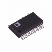
ADM3311EARSZ Analog Devices Inc, ADM3311EARSZ Datasheet - Page 14

ADM3311EARSZ
Manufacturer Part Number
ADM3311EARSZ
Description
IC TXRX RS-232 3:5 2.7V 28SSOP
Manufacturer
Analog Devices Inc
Type
Transceiverr
Datasheet
1.ADM3311EARSZ-REEL.pdf
(24 pages)
Specifications of ADM3311EARSZ
Number Of Drivers/receivers
3/5
Protocol
RS232
Voltage - Supply
2.7 V ~ 3.6 V
Mounting Type
Surface Mount
Package / Case
28-SSOP
Device Type
Transceiver
Ic Interface Type
RS232
No. Of Drivers
1
Supply Voltage Range
2.7V To 3.6V
Driver Case Style
SSOP
No. Of Pins
28
Operating Temperature Range
-40°C To +85°C
Lead Free Status / RoHS Status
Lead free / RoHS Compliant
Available stocks
Company
Part Number
Manufacturer
Quantity
Price
Company:
Part Number:
ADM3311EARSZ
Manufacturer:
ADI
Quantity:
19
Company:
Part Number:
ADM3311EARSZ
Manufacturer:
ADI
Quantity:
9 717
Part Number:
ADM3311EARSZ
Manufacturer:
ADI/亚德诺
Quantity:
20 000
Company:
Part Number:
ADM3311EARSZ-REEL
Manufacturer:
ADI
Quantity:
11 223
Part Number:
ADM3311EARSZ-REEL
Manufacturer:
ADI/亚德诺
Quantity:
20 000
Company:
Part Number:
ADM3311EARSZ-REEL7
Manufacturer:
NEC
Quantity:
100
ADM3307E/ADM3310E/ADM3311E/ADM3312E/ADM3315E
A block diagram of the Green Idle circuit is shown in Figure 26.
Both V+ and V− are monitored and compared to a reference
voltage derived from an on-chip band gap device. If either V+
or V− fall below 7 V
rises above 7.25 V
The operation of Green Idle for V+ under various load
conditions is illustrated in Figure 27. Under light load
conditions, C1 is maintained in a charged condition, and only a
single oscillator pulse is required to charge up C2. Under these
conditions, V+ may actually overshoot 7.25 V
7.25V
7.25V
7.25V
1
2
OSC
OSC
OSC
FOR ADM3310E AND ADM3315E REPLACE WITH 6.5V.
FOR ADM3310E AND ADM3315E REPLACE WITH 6.25V.
7V
7V
7V
V+
V+
V+
1
2
1
2
1
2
SHUTDOWN
Figure 27. Operation of Green Idle under Various Load Conditions
START/STOP
START/STOP
Figure 26. Block Diagram of Green Idle Circuit
OVERSHOOT
2
.
COMPARATOR
COMPARATOR
V+ VOLTAGE
HYSTERESIS
WITH 250mV
V– VOLTAGE
HYSTERESIS
WITH 250mV
1
, the oscillator starts up until the voltage
CHARGE
PUMP
MEDIUM
HEAVY
LIGHT
LOAD
LOAD
LOAD
V+
V–
REFERENCE
BAND GAP
TRANSCEIVERS
VOLTAGE
2
slightly.
Rev. H | Page 14 of 24
Under medium load conditions, it may take several cycles for
C2 to charge up to 7.25 V
oscillator is higher because there are more pulses in each burst
and the bursts of pulses are closer together and more frequent.
Under high load conditions, the oscillator is on continuously if
the charge pump output cannot reach 7.25 V
Green Idle Vs. Shutdown
Shutdown mode minimizes power consumption by shutting
down the charge pump altogether. In this mode, the switches in
the voltage tripler are configured so V+ is connected directly to
V
charge C5. This means there is a delay when coming out of
shutdown mode before V+ and V− achieve their normal
operating voltages. Green Idle maintains the transmitter supply
voltages under transmitter idle conditions so this delay does not
occur.
Doesn’t Green Idle Increase Supply Voltage Ripple?
The ripple on the output voltage of a charge pump operating in
open-loop depends on three factors: the oscillator frequency,
the value of the reservoir capacitor, and the load current. The
value of the reservoir capacitor is fixed. Increasing the oscillator
frequency decreases the ripple voltage; decreasing the oscillator
frequency increases it. Increasing the load current increases the
ripple voltage; decreasing the load current decreases it. The
ripple voltage at light loads is naturally lower than that for high
load currents.
Using Green Idle, the ripple voltage is determined by the high
and low thresholds of the Green Idle circuit. These are
nominally 7 V
load conditions. With very light load conditions, there may be
some overshoot above 7.25 V
Under heavy load conditions where the output never reaches
7.25 V
voltage is determined by the load current, the same as in a
normal charge pump.
What about Electromagnetic Compatibility?
Green Idle does not operate with a constant oscillator
frequency. As a result, the frequency and spectrum of the
oscillator signal vary with load. Any radiated and conducted
emissions also vary accordingly. Like other Analog Devices
RS-232 transceiver products, the ADM33xxE devices feature
slew rate limiting and other techniques to minimize radiated
and conducted emissions.
1
2
For ADM3310E and ADM3315E, replace with 6.5 V.
For ADM3310E and ADM3315E, replace with 6.25 V.
CC
. V− is zero because there is no charge pump operation to
2
, the Green Idle circuit is inoperative and the ripple
1
and 7.25 V
2
. The average frequency of the
2
, so the ripple is 250 mV under most
2
, so the ripple is slightly greater.
2
.


