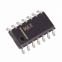
MAX13448EESD+ Maxim Integrated Products, MAX13448EESD+ Datasheet - Page 12

MAX13448EESD+
Manufacturer Part Number
MAX13448EESD+
Description
IC TXRX RS485 FULL DUPLEX 14SOIC
Manufacturer
Maxim Integrated Products
Type
Transceiverr
Datasheet
1.MAX13448EESD.pdf
(14 pages)
Specifications of MAX13448EESD+
Number Of Drivers/receivers
1/1
Protocol
RS485
Voltage - Supply
3 V ~ 5.5 V
Mounting Type
Surface Mount
Package / Case
14-SOIC (3.9mm Width), 14-SOL
Operating Supply Voltage
3 V to 5 V
Supply Current
15 mA
Operating Temperature Range
- 40 C to + 85 C
Data Rate
0.5 Mbps
Mounting Style
SMD/SMT
Propagation Delay Time Ns
700 ns
Lead Free Status / RoHS Status
Lead free / RoHS Compliant
±80V Fault-Protected Full-Duplex
RS-485 Transceiver
receiver threshold between -50mV and -200mV. If the
differential receiver input voltage (A - B) is greater than
or equal to -50mV, RO is logic-high. If A - B is less than
or equal to -200mV, RO is logic-low. In the case of a
terminated bus with all transmitters disabled, the
receiver’s differential input voltage is pulled to 0V by
the termination. With the receiver thresholds of the
MAX13448E, this results in a logic-high with a 50mV
minimum noise margin. The -50mV to -200mV threshold
complies with the ±200mV EIA/TIA-485 standard.
As with all Maxim devices, ESD-protection structures
are incorporated on all pins to protect against electro-
static discharges encountered during handling and
assembly. The driver outputs and receiver inputs of the
MAX13448E have extra protection against static elec-
tricity. Maxim’s engineers have developed state-of-the-
art structures to protect these pins against ESD of ±8kV
without damage. The ESD structures withstand high
ESD in all states: normal operation, shutdown, and
powered down. After an ESD event, the MAX13448E
keeps working without latchup or damage. ESD protec-
tion can be tested in various ways. The transmitter out-
puts and receiver inputs of the MAX13448E are
characterized for protection to the following limits:
• ±8kV using the Human Body Model
ESD performance depends on a variety of conditions.
Contact Maxim for a reliability report that documents
test setup, test methodology, and test results.
Figure 8a shows the Human Body Model, and Figure
8b shows the current waveform it generates when dis-
charged into a low impedance. This model consists of a
Figure 8a. Human Body ESD Test Model
12
VOLTAGE
SOURCE
HIGH-
______________________________________________________________________________________
DC
CHARGE-CURRENT-
LIMIT RESISTOR
1MΩ
R
C
100pF
C s
RESISTANCE
STORAGE
CAPACITOR
DISCHARGE
1500Ω
R
D
±8kV ESD Protection
ESD Test Conditions
Human Body Model
DEVICE
UNDER
TEST
100pF capacitor charged to the ESD voltage of interest,
which is then discharged into the test device through a
1.5kΩ resistor.
Two mechanisms prevent excessive output current and
power dissipation caused by faults or by bus con-
tention. The first, a foldback current limit on the output
stage, provides immediate protection against short
circuits over the whole common-mode voltage range
(see the Typical Operating Characteristics ). The sec-
ond, a thermal-shutdown circuit, forces the driver out-
puts into a high-impedance state if the die temperature
exceeds +160°C (typ).
When circuit boards are inserted into a powered back-
plane, disturbances to the data bus can lead to data
errors. Upon initial circuit-board insertion, the data
communication processor undergoes its own power-up
sequence. During this period, the processor’s logic-
output drivers are high impedance and are unable to
drive the DE input of the device to a defined logic level.
Leakage currents up to ±10µA from the high-imped-
ance state of the processor’s logic drivers could cause
standard CMOS enable inputs of a transceiver to drift to
an incorrect logic level. Additionally, parasitic circuit-
board capacitance could cause coupling of V
GND to the enable inputs. Without the hot-swap capa-
bility, these factors could improperly enable the trans-
ceiver’s driver or receiver.
When V
low. After the initial power-up sequence, the pulldown
circuit becomes transparent, resetting the hot-swap
tolerable input.
Figure 8b. Human Body Current Waveform
AMPS
I
P
CC
36.8%
100%
90%
10%
0
rises, an internal pulldown circuit holds DE
0
t
RL
Driver Output Protection
CURRENT WAVEFORM
TIME
t
DL
Hot-Swap Capability
I r
PEAK-TO-PEAK RINGING
(NOT DRAWN TO SCALE)
Hot-Swap Inputs
CC
or


