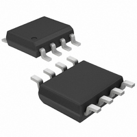
MAX3462ESA+ Maxim Integrated Products, MAX3462ESA+ Datasheet - Page 4

MAX3462ESA+
Manufacturer Part Number
MAX3462ESA+
Description
IC TXRX RS485/422 8-SOIC
Manufacturer
Maxim Integrated Products
Type
Transceiverr
Datasheet
1.MAX3463CSA.pdf
(14 pages)
Specifications of MAX3462ESA+
Number Of Drivers/receivers
1/1
Protocol
RS422, RS485
Voltage - Supply
4.75 V ~ 5.25 V
Mounting Type
Surface Mount
Package / Case
8-SOIC (3.9mm Width)
Data Rate
20000 Kbps
Propagation Delay Time Ns
20 ns
Operating Supply Voltage
5 V
Supply Current
2.5 mA
Operating Temperature Range
- 40 C to + 85 C
Input Voltage
5 V
Maximum Power Dissipation
471 mW
Mounting Style
SMD/SMT
Output Current
+/- 250 mA
Output Voltage
- 8 V to + 13 V
Product
RS-422
Lead Free Status / RoHS Status
Lead free / RoHS Compliant
+5V, Fail-Safe, 20Mbps, Profibus RS-485/
RS-422 Transceivers
ELECTRICAL CHARACTERISTICS (continued)
(V
Note 1: All currents into the device are positive; all currents out of the device are negative. All voltages are referenced to device
Note 2: ∆V
Note 3: The short-circuit output current applies to peak current just prior to foldback-current limiting; the short-circuit foldback output
Note 4: Capacitive load includes test probe and fixture capacitance.
Note 5: Shutdown is enabled by bringing RE high and DE low or by bringing SHDN high. If the enable inputs are in this state for less
(V
4
Receiver Enable from Shutdown to
Output High
Receiver Enable from Shutdown to
Output Low
Time to Shutdown
Driver Enable from Shutdown to
Output High
Driver Enable from Shutdown to
Output Low
CC
CC
2.40
2.35
2.30
2.25
2.20
2.15
2.10
2.05
2.00
_______________________________________________________________________________________
= +5V ±5%, T
= +5V, T
-40
ground, unless otherwise noted.
current applies during current limiting to allow a recovery from bus contention.
than 50ns, the device is guaranteed not to enter shutdown. If the enable inputs are in this state for at least 800ns, the device
is guaranteed to have entered shutdown.
PARAMETER
OD
-20
NO LOAD SUPPLY CURRENT
A
and ∆V
= +25°C, unless otherwise noted.)
vs. TEMPERATURE
DE = V
TEMPERATURE (°C)
0
A
DE = GND
= T
CC
OC
20
MIN
are the changes in V
to T
40
MAX
60
, unless otherwise noted. Typical values are at V
t
t
t
t
SYMBOL
ZH (SHDN)
ZH (SHDN)
ZL (SHDN)
ZL (SHDN)
80
t
SHDN
OD
and V
60
50
40
30
20
10
0
(Note 5)
Figures 8 and 9, R
S2 closed (Note 5)
Figures 8 and 9, R
S1 closed (Note 5)
Figures 8 and 11, R
S2 closed (Notes 4, 5)
Figures 8 and 11, R
S1 closed (Notes 4, 5)
0
vs. RECEIVER OUTPUT LOW VOLTAGE
OC
0.5 1.0
, respectively, when the DI input changes state.
OUTPUT LOW VOLTAGE (V)
OUTPUT CURRENT
1.5
CONDITIONS
2.0
2.5 3.0 3.5 4.0 4.5 5.0
L
L
L
L
= 500Ω, C
= 500Ω, C
Typical Operating Characteristics
= 1kΩ, C
= 1kΩ, C
L
L
L
L
= 15pF,
= 15pF,
= 50pF,
= 50pF,
CC
= +5V and T
35
30
25
20
15
10
5
0
0
MIN
vs. RECEIVER OUTPUT HIGH VOLTAGE
50
A
= +25°C.) (Note 1)
1
OUTPUT HIGH VOLTAGE (V)
OUTPUT CURRENT
TYP
2
MAX
800
3
4
4
4
4
4
UNITS
ns
µs
µs
µs
µs
5


