MC33363BDW ON Semiconductor, MC33363BDW Datasheet
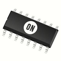
Other Power Management 700V 1.5A Switching

MC33363BDW

Manufacturer Part Number
MC33363BDW
Description
Other Power Management 700V 1.5A Switching
Manufacturer
ON Semiconductor
Type
High Voltage Switching Regulatorr
Datasheet

Specifications of MC33363BDW

Output Voltage Range
5.5 V to 7.5 V
Input Voltage Range
40 V
Mounting Style
SMD/SMT
Package / Case
SOIC-16 Wide
Lead Free Status / Rohs Status
Lead free / RoHS Compliant

Available stocks

Company
Part Number
Manufacturer
Quantity
Price
Part Number:
MC33363BDW
Manufacturer:
ON/安森美
Quantity:
20 000
Part Number:
MC33363BDWG
Manufacturer:
ON
Quantity:
18 435
Part Number:
MC33363BDWR2G
Manufacturer:
ON Semiconductor
Quantity:
3 200
Part Number:
MC33363BDWR2G
Manufacturer:
ON/安森美
Quantity:
20 000
Part Number:
MC33363BDWR2G
Manufacturer:
ON
Quantity:
11 994
MC33363B
High Voltage Switching
Regulator
that is specifically designed to operate from a rectified 240 Vac line
source. This integrated circuit features an on- -chip 700 V/1.0 A
SENSEFET power switch, 500 V active off- -line startup FET, duty
cycle controlled oscillator, current limiting comparator with a
programmable threshold and leading edge blanking, latching pulse
width modulator for double pulse suppression, high gain error
amplifier, and a trimmed internal bandgap reference. Protective
features include cycle- -by- -cycle current limiting, input undervoltage
lockout with hysteresis, overvoltage protection, and thermal
shutdown. This device is available in a 16- -lead dual- -in- -line and wide
body surface mount packages.
Features
*For additional information on our Pb--Free strategy and soldering details, please download the ON Semiconductor Soldering and Mounting
Regulator
 Semiconductor Components Industries, LLC, 2010
November, 2010 - - Rev. 9
R
C
Techniques Reference Manual, SOLDERRM/D.
The MC33363B is a monolithic high voltage switching regulator
T
T
Output
AC Input
On- -Chip 700 V, 1.0 A SENSEFET Power Switch
Rectified 240 Vac Line Source Operation
On- -Chip 500 V Active Off- -Line Startup FET
Latching PWM for Double Pulse Suppression
Cycle- -By- -Cycle Current Limiting
Input Undervoltage Lockout with Hysteresis
Over- -Voltage Protection
Trimmed Internal Bandgap Reference
Internal Thermal Shutdown
These are Pb- -Free Devices*
8
6
7
Thermal
Mirror
PWM
Osc
GND
Figure 1. Simplified Application
4, 5, 12, 13
Reg
PWM Latch
S
R
I
pk
Startup
Q
Startup Input
Driver
EA
LEB
UVLO
1
OVP
V
11
16
10
Overvoltage
Protection
Input
Power Switch
Drain
Compensation
Voltage
Feedback
Input
CC
3
9
1
DC Output
†For information on tape and reel specifications,
MC33363BDWG
MC33363BDWR2G SO--16WB
Regulator Output
16
including part orientation and tape sizes, please
refer to our Tape and Reel Packaging Specification
Brochure, BRD8011/D.
Startup Input
Device
GND
ORDERING INFORMATION
1
V
CC
R
C
A
WL = Wafer Lot
YY = Year
WW = Work Week
G
T
T
PIN CONNECTIONS
http://onsemi.com
DW SUFFIX
CASE 751N
SO- -16WB
1
3
4
5
6
7
8
= Assembly Location
= Pb--Free Package
(Top View)
SO--16WB
(Pb--Free)
(Pb--Free)
Package
Publication Order Number:
16
13
12
10
11
9
1000 Tape & Reel
MC33363BDW
DIAGRAMS
AWLYYWWG
MARKING
Power Switch
Drain
Overvoltage
Protection Input
Voltage Feedback
Input
Compensation
47 Units/Rail
Shipping
GND
MC33363B/D

Related parts for MC33363BDW

MC33363BDW Summary of contents

Page 1

... ORDERING INFORMATION Device Package Shipping MC33363BDWG SO--16WB 47 Units/Rail (Pb--Free) MC33363BDWR2G SO--16WB 1000 Tape & Reel (Pb--Free) †For information on tape and reel specifications, including part orientation and tape sizes, please refer to our Tape and Reel Packaging Specification Brochure, BRD8011/D. Publication Order Number: MC33363B/D † ...

Page 2

MAXIMUM RATINGS (Note 1) Rating Power Switch (Pin 16) Drain Voltage Drain Current Startup Input Voltage (Pin 1, Note 2) Power Supply Voltage (Pin 3) Input Voltage Range Voltage Feedback Input (Pin 10) Compensation (Pin 9) Overvoltage Protection Input (Pin ...

Page 3

ELECTRICAL CHARACTERISTICS for min/max values T is the operating junction temperature range that applies (Note 4), unless otherwise noted.) J Characteristic OVERVOLTAGE DETECTION (Pin 11) Input Threshold Voltage Input Bias Current ( --25 -- 125C) ...

Page 4

100 pF T 500 200 pF T 200 500 1.0 nF 100 2 5 ...

Page 5

V 1.75 V 1.70 V 1.0 ms/DIV Figure 8. Error Amplifier Small Signal Transient Response 0 --20 --40 --60 --80 0 4.0 8 REGULATOR SOURCE CURRENT (mA) reg Figure 10. Regulator Output Voltage Change versus Source ...

Page 6

C = 390 2.0 nF 2.4 T 1.6 0 SUPPLY VOLTAGE (V) CC Figure 14. Supply Current versus Supply Voltage 100 P for T = 50C D(max ...

Page 7

Pin Function 1 Startup Input This pin connects directly to the rectified ac line voltage source. Internally Pin 1 is tied to the drain of a high voltage startup MOSFET. During startup, the MOSFET supplies internal bias, and charges an ...

Page 8

AC Input Current Mirror Regulator Output Band Gap 6.5 V Regulator Oscillator PWM Comparator Thermal Current Limit Shutdown Comparator GND 4, 5, 12, 13 15.2 V 9.5 V ...

Page 9

Introduction The MC33363B represents a new higher level of integration by providing all the active high voltage power, control, and protection circuitry implementation of a flyback or forward converter on a single monolithic chip. This device is designed for direct ...

Page 10

The Power Switch is designed to directly drive the converter transformer and is capable of switching a maximum of 700 V and 1.0 A. Proper device voltage snubbing and heatsinking are required for reliable operation. A Leading Edge Blanking circuit ...

Page 11

... Equal Opportunity/Affirmative Action Employer. This literature is subject to all applicable copyright laws and is not for resale in any manner. PUBLICATION ORDERING INFORMATION LITERATURE FULFILLMENT: Literature Distribution Center for ON Semiconductor P.O. Box 5163, Denver, Colorado 80217 USA Phone: 303--675--2175 or 800--344--3860 Toll Free USA/Canada Fax: 303--675--2176 or 800--344--3867 Toll Free USA/Canada Email: orderlit@onsemi ...

Related keywords