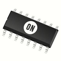
MC33363BDW ON Semiconductor, MC33363BDW Datasheet - Page 7

MC33363BDW
Manufacturer Part Number
MC33363BDW
Description
Other Power Management 700V 1.5A Switching
Manufacturer
ON Semiconductor
Type
High Voltage Switching Regulatorr
Datasheet
1.MC33363BDW.pdf
(11 pages)
Specifications of MC33363BDW
Output Voltage Range
5.5 V to 7.5 V
Input Voltage Range
40 V
Mounting Style
SMD/SMT
Package / Case
SOIC-16 Wide
Lead Free Status / Rohs Status
Lead free / RoHS Compliant
Available stocks
Company
Part Number
Manufacturer
Quantity
Price
Part Number:
MC33363BDW
Manufacturer:
ON/安森美
Quantity:
20 000
Company:
Part Number:
MC33363BDWR2G
Manufacturer:
ON Semiconductor
Quantity:
3 200
Part Number:
MC33363BDWR2G
Manufacturer:
ON/安森美
Quantity:
20 000
Oscillator Output
4, 5, 12, 13
Compensation
Capacitor C
(Power Switch
Blanking Input
Drain Current)
Leading Edge
14, 15
Power Switch
Pin
Comparator
PWM Latch
10
16
11
Gate Drive
1
2
3
6
7
8
9
Q Output
Output
PWM
T
Regulator Output
Protection Input
Feedback Input
Compensation
Power Switch
Startup Input
Overvoltage
Function
Ground
Voltage
Drain
V
R
C
--
CC
--
T
T
This pin connects directly to the rectified ac line voltage source. Internally Pin 1 is tied to the drain of
a high voltage startup MOSFET. During startup, the MOSFET supplies internal bias, and charges an
external capacitor that connects from the V
This pin has been omitted for increased spacing between the rectified ac line voltage on Pin 1 and
the V
This is the positive supply voltage input. During startup, power is supplied to this input from Pin 1.
When V
from an auxiliary transformer winding.
These pins are the control circuit grounds. They are part of the IC lead frame and provide a thermal
path from the die to the printed circuit board.
Resistor R
Comparator threshold and affect the Oscillator frequency.
Capacitor C
programs the Oscillator frequency.
This 6.5 V output is available for biasing external circuitry. It requires an external bypass capacitor of
at least 1.0 mF for stability.
This pin is the Error Amplifier output and is made available for loop compensation. It can be used as
an input to directly control the PWM Comparator.
This is the inverting input of the Error Amplifier. It has a 2.6 V threshold and normally connects
through a resistor divider to the converter output, or to a voltage that represents the converter output.
This input provides runaway output voltage protection due to an external component or connection
failure in the control loop feedback signal path. It has a 2.6 V threshold and normally connects
through a resistor divider to the converter output, or to a voltage that represents the converter output.
These pins have been omitted for increased spacing between the high voltages present on the
Power Switch Drain, and the ground potential on Pins 12 and 13.
This pin is designed to directly drive the converter transformer and is capable of switching a
maximum of 700 V and 1.0 A.
Figure 18. Timing Diagram of Normal Operation
CC
CC
potential on Pin 3.
Normal PWM Operating Range
T
reaches the UVLO upper threshold, the startup MOSFET turns off and power is supplied
T
connects from this pin to ground. The value selected will program the Current Limit
connects from this pin to ground. The value selected, in conjunction with resistor R
PIN FUNCTION DESCRIPTION
http://onsemi.com
7
CC
Description
pin to ground.
Output Overload
Current Limit
Propagation
Delay
2.6 V
0.6 V
Current
Limit
Threshold
T
,


