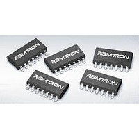
FM32256-G Ramtron, FM32256-G Datasheet

FM32256-G
Specifications of FM32256-G
Available stocks
Related parts for FM32256-G
FM32256-G Summary of contents
Page 1
... DD active when V drops below a programmable DD This product conforms to specifications per the terms of the Ramtron standard warranty. The product has completed Ramtron’s internal qualification testing and has reached production status Rev. 3.1 July 2010 Ferroelectric Nonvolatile RAM • ...
Page 2
... FM3204/16/64/256 Function Event Counter Inputs Device Select inputs Early Power-fail Output Reset Input/Output Early Power-fail Input Serial Data Serial Clock Battery-Backup Supply Supply Voltage Ground Ordering Part Number FM32256-G FM3264-G FM3216-G FM3204-G Page ...
Page 3
A1, A0 Interface SCL SDA LockOut RST PFI + PFO - 1.2V - 2.5V + VDD VBAK Pin Descriptions Pin Name Type Pin Description A0, A1 Input Device select inputs are used to address multiple memories on a serial ...
Page 4
Overview The FM32xx family combines a serial nonvolatile RAM with a processor companion. The companion is a highly integrated peripheral including a processor supervisor, a comparator used for early power-fail warning, nonvolatile event counters, and a 64-bit serial number. The ...
Page 5
The bits VTP1 and VTP0 control the trip point of the low voltage detect circuit. They are located in register 0Bh, bits 1 and 0. V VTP1 VTP0 4.4V 1 ...
Page 6
The voltage on the PFI input pin is compared to an onboard 1.2V reference. When the PFI input voltage drops below this threshold, the comparator will drive the PFO pin to a low state. The comparator has 100 mV (max) ...
Page 7
Although V may be connected to V BAK recommended if the companion is used. None of the companion functions will operate below about 2.5V. Register Map The processor companion functions are accessed via 16 special function registers that are mapped ...
Page 8
Register Description Address Description 18h Serial Number Byte SN.63 SN.62 Upper byte of the serial number. Read/write when SNL=0, read-only when SNL=1. Nonvolatile. 17h Serial Number Byte SN.55 SN.54 Byte 6 of the serial ...
Page 9
Event Counter Control Read Counter. Setting this bit to 1 takes a snapshot of the four counters bytes allowing the system to read the values without missing count events. The RC bit will be ...
Page 10
Watchdog Restart & Flags D7 D6 WTR POR WTR Watchdog Timer Reset Flag: When the /RST signal is activated by the watchdog the WTR bit will be set must be cleared by the user. Note that ...
Page 11
Two-wire Interface The FM32xx employs an industry standard two-wire bus that is familiar to many users. This product is unique since it incorporates two logical devices in one chip. Each logical device can be accessed individually. Although monolithic, it appears ...
Page 12
Slave Address The first byte that the FM32xx expects after a Start condition is the slave address. As shown in figures below, the slave address contains the Slave ID, Device Select address, and a bit that specifies if the transaction ...
Page 13
Stop condition prior to the 8 data bit. The figures below illustrate a single- and multiple-writes to Start By Master S Slave Address By FM32xx Start By Master S Slave Address FM32xx Memory Read Operation ...
Page 14
To perform a selective read, the bus master sends out the slave address with the LSB set to 0. This specifies a write operation. ...
Page 15
... Addressing FRAM Array in the FM32xx Family The FM32xx family includes 256Kb, 64Kb, 16Kb, and 4Kb memory densities. The following 2-byte address field is shown for each density. Table 4. Two-Byte Memory Address st Part # 1 FM32256 x A14 A13 FM3264 ...
Page 16
Electrical Specifications Absolute Maximum Ratings Symbol V Power Supply Voltage with respect Voltage on any signal pin with respect Backup Supply Voltage BAK T Storage Temperature STG T Lead Temperature (Soldering, 10 ...
Page 17
... The minimum V to guarantee the level of /RST remains a valid Full complete operation. Supervisory circuits operate to lower voltages as specified. 8. Includes /RST input detection of external reset condition to trigger driving of /RST signal by FM32xx. 9. The VBAK trickle charger automatically regulates the maximum voltage on this pin for capacitor backup applications. ...
Page 18
Supervisor Timing (T = -40° 85° Symbol Parameter t /RST Active (low) after V RPU t V < V Noise Immunity RNR Rise Time Fall Time ...
Page 19
AC Test Conditions Input Pulse Levels Input rise and fall times Input and output timing levels Diagram Notes All start and stop timing parameters apply to both read and write cycles. Clock specifications are identical for read and write cycles. ...
Page 20
... SOIC Package Marking Scheme Legend: XXXXXXX-P LLLLLLL RIC YYWW Example: FM32256, “Green” SOIC package, Year 2009, Work Week 42 Rev. 3.1 July 2010 XXXX= part number, P= package type (-G) LLLLLLL= lot code RIC=Ramtron Int’l Corp, YY=year, WW=work week FM32256-G B90007G RIC 0942 FM3204/16/64/256 Page ...
Page 21
Revision History Revision Date Summary 0.2 5/22/03 0.21 11/25/03 Fixed package drawing dimensions. 1.0 3/30/04 Operating table. Changed V 2.0 10/25/04 Changed to Pre-Production status. Added text to Trickle Charger section. Improved spec limits on V limits in DC Operating ...


