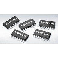
FM32256-G Ramtron, FM32256-G Datasheet - Page 7

FM32256-G
Manufacturer Part Number
FM32256-G
Description
Supervisory Circuits 256K w/Pwr Mon WDT Bat Sw Pwr Fail
Manufacturer
Ramtron
Datasheet
1.FM3264-G.pdf
(21 pages)
Specifications of FM32256-G
Number Of Voltages Monitored
4
Monitored Voltage
2.6 V, 2.9 V, 3.9 V, 4.4 V
Output Type
Active Low, Bidirectional
Manual Reset
Resettable
Watchdog
Watchdog
Battery Backup Switching
Backup
Power-up Reset Delay (typ)
200 ms
Supply Voltage (max)
5.5 V
Supply Voltage (min)
2.7 V
Supply Current (typ)
1500 uA
Maximum Operating Temperature
+ 85 C
Mounting Style
SMD/SMT
Package / Case
SOIC-14
Minimum Operating Temperature
- 40 C
Power Fail Detection
Yes
Lead Free Status / Rohs Status
Lead free / RoHS Compliant
Available stocks
Company
Part Number
Manufacturer
Quantity
Price
Company:
Part Number:
FM32256-GTR
Manufacturer:
CYPRESS
Quantity:
681
Although V
recommended if the companion is used. None of the
companion functions will operate below about 2.5V.
Register Map
The processor companion functions are accessed via 16 special function registers that are mapped to a separate 2-
wire device ID. The interface protocol is described below. The registers contain control bits, or information flags. A
description of each register follows.
Register Map Summary Table
Nonvolatile =
*Note that the usable address range starts at address 09h to preserve software compatibility with the FM31xx
device family, which includes a real-time clock in registers 00-08h.
Note: When the device is first powered up and programmed, all registers must be written because the battery-
backed register values cannot be guaranteed. The table below shows the default values of the non-volatile
registers. All other register values should be treated as unknown.
Rev. 3.1
July 2010
Address
00-08h
0Dh
0Ch
0Fh
0Eh
0Bh
0Ah
18h
17h
16h
15h
14h
13h
12h
11h
10h
09h
BAK
WDE
WTR
SNL
D7
-
may be connected to V
POR
D6
-
-
-
Battery-backed =
D5
LB
-
-
-
Serial Number Byte 7
Serial Number Byte 6
Serial Number Byte 5
Serial Number Byte 4
Serial Number Byte 3
Serial Number Byte 2
Serial Number Byte 1
Serial Number Byte 0
Counter 2 MSB
Counter 1 MSB
Counter 2 LSB
Counter 1 LSB
SS
WDT4
WP1
, this is not
D4
DO NOT USE
-
-
Default Register Values
Address
Data
18h
17h
16h
15h
14h
13h
12h
11h
0Bh
0Ah
WDT3
WP0
WR3
RC
D3
Hex Value
0x00
0x00
0x00
0x00
0x00
0x00
0x00
0x00
0x00
0x1F
WDT2
WR2
VBC
CC
D2
the VBC bit to 0 to prevent battery charging. The
V
resistor as a safety element.
BAK
Note: systems using lithium batteries should clear
circuitry includes an internal 1 K
WDT1
VTP1
WR1
C2P
D1
WDT0
VTP0
WR0
C1P
D0
Function
Companion Control
Serial Number 7
Serial Number 6
Serial Number 5
Serial Number 4
Serial Number 3
Serial Number 2
Serial Number 1
Serial Number 0
Event Counter 2 MSB
Event Counter 2 LSB
Event Counter 1 MSB
Event Counter 1 LSB
Event Count Control
Watchdog Control
Watchdog Restart/Flags
RESERVED
FM3204/16/64/256
Page 7 of 21
Ω
Range
FFh
FFh
FFh
FFh
FFh
FFh
FFh
FFh
FFh
FFh
FFh
FFh
series


