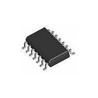
PS10NG Supertex, PS10NG Datasheet - Page 5

PS10NG
Manufacturer Part Number
PS10NG
Description
Supervisory Circuits Quad Pwr Seq Cntlr
Manufacturer
Supertex
Datasheet
1.PS10NG.pdf
(9 pages)
Specifications of PS10NG
Number Of Voltages Monitored
4
Manual Reset
Not Resettable
Watchdog
No Watchdog
Supply Voltage (max)
- 10 V
Supply Voltage (min)
- 90 V
Supply Current (typ)
450 uA
Maximum Power Dissipation
750 mW
Maximum Operating Temperature
+ 85 C
Mounting Style
SMD/SMT
Package / Case
SO-14
Minimum Operating Temperature
- 40 C
Lead Free Status / Rohs Status
Lead free / RoHS Compliant
Then:
(V
(V
And:
(V
(V
Therefore, the circuit will start when the input supply voltage
is in the range of 38.45V to 60.51V.
Undervoltage/Overvoltage Protection
t
active. It can be approximated by:
t
where:
C
V
I
PWRGD-A
PWRGD-A
RAMP
INT
RAMP
EEUV(on)
EEUV(on)
EEOV(on)
EEOV(on)
OV
UV
GND
UV
OV
= internal regulated power supply voltage (10V typ.)
= 10µA charge current
V
= capacitor connected from RAMP pin to VEE pin
OFF
OFF
ON
ON
IN
= C
is the time delay from V
) = 1.22 x (R1+R2+R3)/(R2+R3)
) = 1.22 x (487k+6.65k+9.31k)/(6.65k+9.31k)
) = 1.12 x (R1+R2+R3)/R3
) = 1.12 x (487kΩ +6.65kΩ +9.31kΩ)/9.31kΩ
= 38.45V
= 60.51V
RAMP
PWRGD
x (V
INT
-1.17)/I
SET
RAMP
RESET
EEUV(on)
to PWRGD-A going
5
PWRGD Flags Delay Programming
When the ramp voltage hits V
comes active indicating that the input supply voltage is within
the programmed limits. PWRGD-B goes active after a pro-
grammed time delay after PWRGD-A went active. PWRGD-
C goes active after a programmed time delay after PWRGD-
B went active. PWRGD-D goes active after a programmed
time delay after PWRGD-C went active.
The resistors connected from TB, TC, and TD to VEE pin
determines the delay times between the PWRGD fl ags.
The value of the resistors determines the capacitor charging
and discharging current of a triangular wave oscillator. The
oscillator output is fed into an 8-bit counter to generate the
desired time delay.
The respective time delay is defi ned by the following equa-
tion:
t
and
I
Where:
t
C
V
I
V
R
Combining the two equations and solving for R
R
For a time delay of 200ms
R
For a time delay of 5ms
R
TX
CD
TX
CD
PP
BG
TX
TX
TX
TX
OSC
= (255 x 2 x C
= Time delay between respective PWRGD fl ags
= V
= Charge and discharge current of oscillator
= 0.585 x 10⁶ x t
= 8.2V (peak-to-peak voltage swing of oscillator)
= Programming resistor at TB, TC, or TD
= (V
= 1.17V (internal band gap reference)
= 120pF (internal oscillator capacitor)
BG
BG
= 0.585 x 106 x 0.2 = 117kΩ
= 0.585 x 106 x 0.005 = 2.925kΩ
/ (4 x R
x t
TX
) / (2040 x C
TX
OSC
)
x V
TX
PP
)/I
OSC
CD
x V
INT
PP
- 1.17V, PWRGD-A be-
)
TX
yields:
PS10


