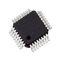
MC100EP445FA ON Semiconductor, MC100EP445FA Datasheet

MC100EP445FA
Specifications of MC100EP445FA
Available stocks
Related parts for MC100EP445FA
MC100EP445FA Summary of contents
Page 1
... CLK ENABLE Immune to Runt Pulse Generation • Pb−Free Packages are Available* *For additional information on our Pb−Free strategy and soldering details, please download the ON Semiconductor Soldering and Mounting Techniques Reference Manual, SOLDERRM/D. © Semiconductor Components Industries, LLC, 2010 September, 2010 − Rev ...
Page 2
RESET 1 SYNC 2 CKEN 3 CLK 4 CLK 5 V BB1 6 CKSEL Warning: All V Power Supply to guarantee proper operation. Figure 1. 32−Lead LQFP Pinout (Top View) V SINA SINA V V ...
Page 3
Table 2. TRUTH TABLE PIN SINSEL Select SINB Input CKSEL Q: PCLK = 8:1 CLK 1:1 CLK Q CKEN Synchronously Disable Internal Clock Circuitry RESET Asynchronous Master Reset SYNC Asynchronously Applied to Swallow a Data Bit SINA V ...
Page 4
Table 3. ATTRIBUTES Internal Input Pulldown Resistor Internal Input Pull−up Resistor ESD Protection Moisture Sensitivity, Indefinite Time Out of Drypack (Note 1) Flammability Rating Transistor Count Meets or exceeds JEDEC Spec EIA/JESD78 IC Latchup Test 1. For additional information, see ...
Page 5
Table 5. 10EP DC CHARACTERISTICS, PECL Symbol Characteristic I Power Supply Current EE V Output HIGH Voltage (Note Output LOW Voltage (Note Input HIGH Voltage (Single−Ended Input LOW Voltage (Single−Ended ...
Page 6
Table 7. 10EP DC CHARACTERISTICS, NECL Symbol Characteristic I Power Supply Current (Note 10 Output HIGH Voltage (Note 11 Output LOW Voltage (Note 11 Input HIGH Voltage (Single−Ended Input LOW Voltage (Single−Ended) ...
Page 7
Table 9. 100EP DC CHARACTERISTICS, PECL Symbol Characteristic I Power Supply Current (Note 17 Output HIGH Voltage (Note 18 Output LOW Voltage (Note 18 Input HIGH Voltage (Single−Ended Input LOW Voltage (Single−Ended) ...
Page 8
Table 11. AC CHARACTERISTICS V Symbol Characteristic f Maximum Input CLK Frequency max (See Figure 13. F /JITTER) max t , Propagation Delay to PLH t Output Differential PHL ts Setup Time SINA CLK+ (Figure 5) CKEN+ TO ...
Page 9
Reset CLK CLK Figure 4. Reset Recovery CLK Data Setup Time + Data Hold Time − Figure 5. Data Setup and Hold Time CLK + CKEN Setup Time CKEN Hold Time − Figure 6. CKEN Setup and Hold Time http://onsemi.com ...
Page 10
The MC10/100EP445 is an integrated 1:8 serial to parallel converter with two modes of operation selected by CKSEL (Pin 7). CKSEL HIGH mode only latches data on the rising edge of the input CLK and CKSEL LOW mode latches data ...
Page 11
For CKSEL LOW operation, the data is latched on both the rising edge and the falling edge of the clock and the time from when the serial data is latchedÀ to when the data is seen on the parallel outputÁ ...
Page 12
Similarly, for CKSEL HIGH operation, the data is latched only on the rising edge of the clock and the time from when the serial data is latchedÀ to when the data is seen on the parallel outputÁ clock ...
Page 13
To allow the user to synchronize the output byte data correctly, the start bit for conversion can be moved using the SYNC input pin (pin 2). Asynchronously asserting the SYNC pin will force the internal clock to swallow a clock ...
Page 14
For CKSEL HIGH, a single pulse applied asynchronously for three consecutive clock cycles shifts the start bit for conversion from The bit is swallowed following n n−1 the three clock cycle pulse width of SYNCÀ on ...
Page 15
The synchronous CKEN (pin 3) applied with at least one clock cycle pulse length will disable the internal clock signal. The synchronous CKEN will suspend all of the device activities and prevent runt pulses from being generated. The rising edge ...
Page 16
CKSEL LOW 600 500 400 300 200 (JITTER) É É É É É É É É É É É É É É É É 100 É É É É É É É É É É É ...
Page 17
... MC10EP445FA MC10EP445FAG MC10EP445FAR2 MC10EP445FAR2G MC10EP445MNG MC10EP445MNR4G MC100EP445FA MC100EP445FAG MC100EP445FAR2 MC100EP445FAR2G MC100EP445MNG MC100EP445MNR4G †For information on tape and reel specifications, including part orientation and tape sizes, please refer to our Tape and Reel Packaging Specifications Brochure, BRD8011/D. Resource Reference of Application Notes AN1405/D AN1406/D AN1503/D ...
Page 18
−T− DETAIL −Z− −AB− −AC− SEATING PLANE 0.10 (0.004) AC NOTES: 1. DIMENSIONING AND TOLERANCING PER ANSI Y14.5M, 1982. 2. CONTROLLING DIMENSION: MILLIMETER. 3. DATUM PLANE ...
Page 19
... X 0.28 *For additional information on our Pb−Free strategy and soldering details, please download the ON Semiconductor Soldering and Mounting Techniques Reference Manual, SOLDERRM/D. N. American Technical Support: 800−282−9855 Toll Free USA/Canada Europe, Middle East and Africa Technical Support: Phone: 421 33 790 2910 Japan Customer Focus Center Phone: 81− ...


