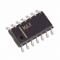
MAX3292ESD+ Maxim Integrated Products, MAX3292ESD+ Datasheet - Page 7

MAX3292ESD+
Manufacturer Part Number
MAX3292ESD+
Description
IC TXRX RS485/422 10MBPS 14-SOIC
Manufacturer
Maxim Integrated Products
Type
Transceiverr
Datasheet
1.MAX3292EPD.pdf
(16 pages)
Specifications of MAX3292ESD+
Number Of Drivers/receivers
1/1
Protocol
RS422, RS485
Voltage - Supply
4.75 V ~ 5.25 V
Mounting Type
Surface Mount
Package / Case
14-SOIC (3.9mm Width), 14-SOL
Operating Supply Voltage
5 V
Mounting Style
SMD/SMT
Product
RS-422/RS-485 Combination
Lead Free Status / RoHS Status
Lead free / RoHS Compliant
Figure 1. Driver DC Test Load
MAX3291
6, 8, 13
—
10
11
12
—
14
1
2
3
4
5
7
9
for High-Speed, Long-Distance Communication
RS-485/RS-422 Transceivers with Preemphasis
PIN
MAX3292
Y
Z
6, 7
10
11
12
13
14
—
1
2
3
4
5
8
9
_______________________________________________________________________________________
V
V
OD
ODP
NAME
V
PSET
GND
N.C.
PEE
V
RO
DE
RE
CCD
DI
Y
Z
B
A
CC
R
R
V
OC
Preemphasis Enable Input. To enable preemphasis, leave PEE unconnected, connect to
V
low.
Preemphasis Set Input. Sets the preemphasis interval. Connect a resistor (R
lel with a capacitor (C
Operating Circuit .
Receiver Output. When RE is low and if A - B ≥ 200mV, RO is high; if A - B ≤ -200mV, RO
is low.
Receiver Output Enable. Drive RE low to enable RO; RO is high impedance when RE is
high. Drive RE high and DE low to enter low-power shutdown mode.
Driver Output Enable. Drive DE high to enable the driver outputs. These outputs are high
impedance when DE is low. Drive RE high and DE low to enter low-power shutdown mode.
Driver Input. With DE high, a low on DI forces the noninverting output low and the inverting
output high. Similarly, a high on DI forces the noninverting output high and the inverting
output low.
No Connection. Not internally connected.
Ground
Noninverting Driver Output
Inverting Driver Output
Inverting Receiver Input
Noninverting Receiver Input
Connect to V
Positive Supply: +4.75V ≤ V
CC
, or drive high. To enable strong-level-drive only mode, connect PEE to GND or drive
CC
PSET
) from PSET to V
CC
Figure 2. Driver or Receiver Enable/Disable Timing Test Load
≤ +5.25V
UNDER TEST
OUTPUT
FUNCTION
CC
to set the preemphasis interval. See Typical
C
L
R
L
Pin Description
S1
S2
PSET
) in paral-
V
CC
7


