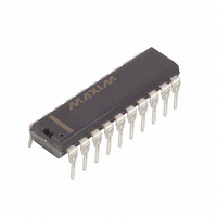
DS229 Maxim Integrated Products, DS229 Datasheet

DS229
Specifications of DS229
Available stocks
Related parts for DS229
DS229 Summary of contents
Page 1
... Additional 12-volt supplies are not needed since the DS229 uses on-board charge pumps to convert the +5-volt supply to 10 volts. The DS229 is fully compliant with EIA RS-232E and V.28/V.24 standards. The DS229 contains three drivers and three receivers. Driver slew rates and data rates are guaranteed up to 116 kbits/sec ...
Page 2
... FUNCTIONAL DIAGRAM OF DS229 Figure 1 NOTE recommended decoupling capacitor which is the same value as C1, C2, C3, and C4. PIN DESCRIPTIONS V , GND: DC power is provided to the device on these pins V+: Positive supply output (RS-232). V+ requires an external storage charge capacitor of at least 0 larger capacitor ( can be used to reduce supply ripple. ...
Page 3
... V+. Likewise, C2 can be omitted if -12V is connected directly to V-. DUAL CHARGE PUMP CONVERTERS The DS229 has a two stage on-board charge pump circuit that is used to generate 10 volts from a single +5-volt supply. In the first stage, capacitor C1 doubles the +5V supply to +10 volts which is then stored on capacitor C3 ...
Page 4
... CC 30V (V+ + 0.3V) to (V- - 0.3V) -0. 0.3V) CC Continuous SYMBOL MIN TYP V 4.5 CC SYMBOL MIN TYP I 6 CC1 I 22.5 CC2 ORS V 0.8 1.4 TTL V 1.4 TTH f 200 300 10M OUT TSC DS229 ( MAX UNITS NOTES 5 MAX UNITS NOTES 2.0 V 116 kbits 100 ...
Page 5
... IR V 0.8 RTL V RTH V 0 ROL V 3.5 ROH I -2 RSC I 10 RSC SYMBOL MIN PHLT t PLHT t PHLR t PLHR t PHLT -t PLHT t PHLR -t PLHR = 2V 1.3 V 1.8 2 0 TYP MAX UNITS NOTES 1.3 3.5 s 1.5 3 300 ns 100 ns DS229 ...
Page 6
... TRANSMITTER PROPAGATION DELAY TIMING Figure 2 RECEIVER PROPAGATION DELAY TIMING Figure DS229 ...
Page 7
... C IN. 0.120 0.140 MM 3.05 3.56 D IN. 0.295 0.325 MM 7.49 8.26 E IN. 0.015 0.040 MM 0.38 1.02 F IN. 0.120 0.140 MM 3.04 3.56 G IN. 0.090 0.110 MM 2.23 2.79 H IN. 0.310 0.390 MM 7.87 9.91 J IN. 0.008 0.012 MM 0.20 0.30 K IN. 0.015 0.021 MM 0.38 0. DS229 ...
Page 8
... A2 IN. 0.089 0.095 MM 2.26 2.41 b IN. 0.013 0.020 MM 0.33 0.51 C IN. 0.009 0.013 MM 0.229 0.33 D IN. 0.498 0.511 MM 12.65 12.99 e IN. 0.050 BSC MM 1.27 BSC E1 IN. 0.290 0.300 MM 7.37 7.62 H IN. 0.398 0.416 MM 10.11 10.57 L IN. 0.016 0.040 MM 0.40 1. DS229 ...
Page 9
... TSSOP DIM MIN MAX 1. 0. 0.75 1. 0.09 0. 0.50 0. 0.65 BSC B MM 0.18 0. 6.40 6. 4.40 NOM G MM 0.25 REF H MM 6.25 6.55 phi DS229 ...


