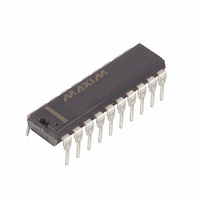
DS229 Maxim Integrated Products, DS229 Datasheet - Page 3

DS229
Manufacturer Part Number
DS229
Description
IC TXRX TRI 5V RS-232 20-DIP
Manufacturer
Maxim Integrated Products
Type
Transceiverr
Datasheet
1.DS229SN.pdf
(9 pages)
Specifications of DS229
Number Of Drivers/receivers
3/3
Protocol
RS232
Voltage - Supply
4.5 V ~ 5.5 V
Mounting Type
Through Hole
Package / Case
20-DIP (0.300", 7.62mm)
Lead Free Status / RoHS Status
Contains lead / RoHS non-compliant
Available stocks
Company
Part Number
Manufacturer
Quantity
Price
Part Number:
DS229E
Manufacturer:
DALLAS
Quantity:
20 000
Part Number:
DS229S
Manufacturer:
DALLAS
Quantity:
20 000
V-: Negative supply output (RS-232). V- requires an external storage capacitor of at least 0.1 F. A
larger capacitor (up to 10 F) can be used to reduce supply ripple.
T1
be left unconnected since each input has a 400 k pullup resistor.
T1
loads up to 3 k . These driver outputs provide current necessary to meet RS-232 levels for loads up to
2500 pF.
R1
5 k terminating resistor. Each receiver provides 0.5V hysteresis (typical) for noise immunity.
R1
C1+, C1-, C2+, C2-: Charge pump capacitor inputs. These pins require two external capacitors (0.1 F
minimum, 10 F maximum and should be the same size as C3 and C4). Capacitor 1 is connected between
C1+ and C1-. Capacitor 2 is connected between C2+ and C2-. Capacitor C1 can be omitted if +12 volts is
connected directly to V+. Likewise, C2 can be omitted if -12V is connected directly to V-.
DUAL CHARGE PUMP CONVERTERS
The DS229 has a two stage on-board charge pump circuit that is used to generate 10 volts from a single
+5-volt supply. In the first stage, capacitor C1 doubles the +5V supply to +10 volts which is then stored
on capacitor C3. The second stage uses capacitor C2 to invert the +10V potential to -10V. This charge is
then stored on capacitor C4. The 10-volt supplies allow the DS229 to provide the necessary output
levels for RS-232 communication. The DS229 will operate with charge pump capacitors as low as 0.1
RS-232 DRIVERS
The three RS-232 drivers are powered by the internal 10-volt supplies generated by the on-board charge
pump. The driver inputs are both TTL and CMOS compatible. Each input has an internal 400 k =pullup
resistor so that unused transmitter inputs can be left unconnected. The open circuit output voltage swing
is from (V+ - 0.6) to V- volts. Worst case conditions for EIA-232E/V.28 of 5 volts driving a 3 k =load
and 2500 pF are met at maximum operating temperature and V
swings of 8 volts occur when loaded with a nominal 5 k =RS-232 receiver. As required by EIA-232E
and V.28 specifications, the slew rate at the output is limited to less than 30 volts/ s. Typical slew rates
are 20 volts/ s unloaded and 12 volts/ s with 3 k =and 2500 pF load. These slew rates allow for bit rates
of over 116 kbits/s. Driver outputs maintain high impedance when power is off.
RS-232 RECEIVERS
The three receivers conform fully to the RS-232E specifications. The input impedance is typically 5
k =and can withstand up to 30 volts with or without V
within the 3-volt limit of RS-232E specification with an input threshold low of 0.8 volts and an input
threshold high of 2.4 volts. The receivers have 0.5 volts of hysteresis (typical) to improve noise rejection.
The TTL/CMOS compatible outputs of the receivers will be low whenever the RS-232 input is greater
than 2.4 volts. The receiver output will be high when the input is floating or driven between +0.8 volts
and -25 volts.
F. Larger capacitors (up to 10 F) can be used to reduce supply ripple.
IN
OUT
IN
OUT
, T2
, R2
, T2
, R2
IN
IN
, T3
OUT
OUT
, R3
, T3
, R3
IN
IN
: Standard TTL/CMOS inputs for the RS-232 drivers. The inputs of unused drivers can
: Receiver inputs. These inputs accept RS-232 level signals (±25 volts) into a protected
OUT
OUT
: Receiver outputs at TTL/CMOS levels.
: Driver outputs at RS-232 levels. Driver output swing meets RS-232 levels for
3 of 9
CC
applied. The input switching thresholds are
CC
equal to 4.5 volts. Typical voltage
DS229


