ALD2722PB Advanced Linear Devices Inc, ALD2722PB Datasheet
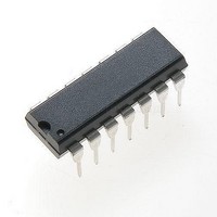
Op Amps 5V High Precision

ALD2722PB

Manufacturer Part Number
ALD2722PB
Description
Op Amps 5V High Precision
Manufacturer
Advanced Linear Devices Inc
Datasheet

Specifications of ALD2722PB

Number Of Channels
2
Voltage Gain Db
107.96 dB
Common Mode Rejection Ratio (min)
90 dB
Input Offset Voltage
0.12 mV
Operating Supply Voltage
5 V, 9 V
Supply Current
3 mA
Maximum Power Dissipation
15 mW
Maximum Operating Temperature
+ 70 C
Mounting Style
Through Hole
Package / Case
PDIP-14
Maximum Dual Supply Voltage
+/- 5 V
Minimum Operating Temperature
0 C
Lead Free Status / Rohs Status
No
* Contact factory for industrial temperature range
© 1998 Advanced Linear Devices, Inc. 415 Tasman Drive, Sunnyvale, California 94089 -1706 Tel: (408) 747-1155 Fax: (408) 747-1286 http://www.aldinc.com
KEY FEATURES
• 5V single supply operation
• EPAD ( Electrically Programmable Analog Device)
• User programmable V
• Computer-assisted trimming
• Rail-to-rail input/output
• Compatible with standard EPAD Programmer
• Each amplifier V
• High precision through in-system circuit trimming
• Reduces or eliminates V
• System level “calibration” capability
• Application Specific Programming mode
• In-System Programming mode
• Electrically programmable to compensate for
• Achieves 0.01pA input bias current and 25 V
ORDERING INFORMATION
GENERAL DESCRIPTION
The ALD2722E/ALD2722 is a dual monolithic rail-to-rail precision CMOS
operational amplifier with integrated user programmable EPAD (Electri-
cally Programmable Analog Device) based offset voltage adjustment. The
ALD2722E/ALD2722 is a dual version of the ALD1722E/ALD1722 opera-
tional amplifier. Each ALD2722E/ALD2722 operational amplifier features
individual, user-programmable offset voltage trimming resulting in signifi-
cantly enhanced total system performance and user flexibility.
technology is an exclusive ALD design which has been refined for analog
applications where precision voltage trimming is necessary to achieve a
desired performance. It utilizes CMOS FETs as in-circuit elements for
trimming of offset voltage bias characteristics with the aid of a personal
computer under software control. Once programmed, the set parameters
are stored indefinitely. EPAD offers the circuit designer a convenient and
cost-effective trimming solution for achieving the very highest amplifier/
system performance.
The ALD2722E/ALD2722 dual operational amplifier features rail-to-rail
input and output voltage ranges, tolerance to overvoltage input spikes of
300mV beyond supply rails, high capacitive loading up to 4000pF, ex-
tremely low input currents of 0.01pA typical, high open loop voltage gain,
useful bandwidth of 1.5MHz, slew rate of 1.9V/ s, and low typical supply
current of 2mA for both amplifiers.
external component tolerances
input offset voltage
-55 C to +125 C
14-Pin
CERDIP
Package
ALD2722E DB
ALD2722 DB
A
L
D
INEAR
DVANCED
EVICES,
OS
Operating Temperature Range
I
can be trimmed to a different Vos level
NC.
OS
0 C to +70 C
14-Pin
Small Outline
Package (SOIC)
ALD2722E SB
ALD2722 SB
OS
trimmer
, PSRR, CMRR and TCV
DUAL EPAD™ OPERATIONAL AMPLIFIER
0 C to +70 C
Plastic Dip
ALD2722E PB
ALD2722 PB
14-Pin
Package
OS
errors
EPAD
BENEFITS
• Eliminates manual and elaborate
• Remote controlled automated trimming
• In-System Programming capability
• No external components
• No internal clocking noise source
• Simple and cost effective
• Small package size
• Extremely small total functional
• Low system implementation cost
• Micropower
APPLICATIONS
• Sensor interface circuits
• Transducer biasing circuits
• Capacitive and charge integration circuits
• Biochemical probe interface
• Signal conditioning
• Portable instruments
• High source impedance electrode
• Precision Sample and Hold amplifiers
• Precision current to voltage converter
• Error correction circuits
• Sensor compensation circuits
• Precision gain amplifiers
• Periodic In-system calibration
• System output level shifter
PIN CONFIGURATION
+IN
+IN
amplifiers
-IN
-IN
system trimming procedures
volume size
N/C
N/C
V -
A
A
B
B
4
5
1
6
2
3
7
DB, PB, SB PACKAGE
TOP VIEW
ALD2722E/ALD2722
14
13
12
11
10
9
8
VE
VE
VE
VE
OUT
V +
OUT
2A
1A
1B
2B
A
B

Related parts for ALD2722PB

ALD2722PB Summary of contents

Page 1

A DVANCED L INEAR D I EVICES, NC. KEY FEATURES • 5V single supply operation • EPAD ( Electrically Programmable Analog Device) • User programmable V trimmer OS • Computer-assisted trimming • Rail-to-rail input/output • Compatible with standard EPAD Programmer ...

Page 2

FUNCTIONAL DESCRIPTION The ALD2722E/ALD2722 utilizes EPADs as in-circuit elements for trimming of offset voltage bias characteristics. Each ALD2722E/ALD2722 operational amplifier has a pair of EPAD-based circuits connected such that one circuit is used to adjust V in one direction and ...

Page 3

ABSOLUTE MAXIMUM RATINGS + Supply voltage, V Differential input voltage range Power dissipation Operating temperature range Storage temperature range Lead temperature, 10 seconds OPERATING ELECTRICAL CHARACTERISTICS 2.5V unless otherwise specified A S Parameter ...

Page 4

OPERATING ELECTRICAL CHARACTERISTICS (cont' 2.5V unless otherwise specified A S Parameter Symbol Supply Current I S Power Dissipation P D Input Capacitance C IN Maximum Load Capacitance C L Equivalent Input Noise Voltage ...

Page 5

V = 2.5V - +125 C unless otherwise specified S A Parameter Initial Input offset Voltage Input Offset Current Input Bias Current Initial Power Supply Rejection Ratio 8 Initial Common Mode Rejection Ratio 8 Large Signal Voltage Gain ...

Page 6

TYPICAL PERFORMANCE CHARACTERISTICS COMMON MODE INPUT VOLTAGE RANGE AS A FUNCTION OF SUPPLY VOLTAGE SUPPLY VOLTAGE (V) INPUT BIAS CURRENT AS A ...

Page 7

TYPICAL PERFORMANCE CHARACTERISTICS OUTPUT VOLTAGE SWING AS A FUNCTION OF SUPPLY VOLTAGE 125 10K 10K SUPPLY VOLTAGE (V) OPEN ...

Page 8

TWO EXAMPLES OF EQUIVALENT INPUT OFFSET VOLTAGE DUE TO 500 400 300 200 100 THREE EXAMPLES OF EQUIVALENT INPUT OFFSET VOLTAGE DUE TO CHANGE IN COMMON MODE VOLTAGE vs. COMMON MODE VOLTAGE 500 400 300 EXAMPLE B: ...

Page 9

APPLICATION SPECIFIC / IN-SYSTEM PROGRAMMING Examples of applications where accumulated total input offset voltage from various contributing sources is minimized under different sets of user-specified operating conditions 2500 2000 1500 V BUDGET AFTER OS 1000 EPAD PROGRAMMING 500 0 -500 ...

Page 10

DEFINITIONS AND DESIGN NOTES: 1. Initial Input Offset Voltage is the initial offset voltage of the ALD2722E/ALD2722 operational amplifier when shipped from the factory. The device has been pre-programmed and tested for programmability. 2. Offset Voltage Program Range is the ...

Related keywords