ALD2724SB Advanced Linear Devices Inc, ALD2724SB Datasheet
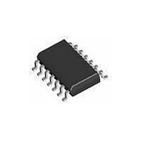
Op Amps High Slew Rate

ALD2724SB

Manufacturer Part Number
ALD2724SB
Description
Op Amps High Slew Rate
Manufacturer
Advanced Linear Devices Inc
Datasheet

Specifications of ALD2724SB

Number Of Channels
2
Voltage Gain Db
87.96 dB
Common Mode Rejection Ratio (min)
90 dB
Input Offset Voltage
0.15 mV
Operating Supply Voltage
9 V
Supply Current
6.5 mA
Maximum Power Dissipation
65 mW
Maximum Operating Temperature
+ 70 C
Mounting Style
SMD/SMT
Package / Case
SOIC-14
Maximum Dual Supply Voltage
+/- 5.25 V
Minimum Operating Temperature
0 C
Lead Free Status / Rohs Status
No
GENERAL DESCRIPTION
The ALD2724E/ALD2724 is a dual monolithic operational amplifier with
MOSFET input that has rail-to-rail input and output voltage ranges. The
input voltage range and output voltage range are very close to the positive
and negative power supply voltages. Typically the input voltage can be
beyond positive power supply voltage V + or the negative power supply
voltage V - by up to 300mV. The output voltage swings to within 60mV of
either positive or negative power supply voltages at rated load.
With high impedance load, the output voltage of the ALD2724E/ALD2724
approaches within 1mV of the power supply rails. This device is designed
as an alternative to the popular J-FET input operational amplifier in
applications where lower operating voltages, such as 9V battery or 3.25V
to 5V power supplies are being used. The ALD2724E/ALD2724 offers
high slew rate of 5.0V/ s.
The rail-to-rail input and output feature of the ALD2724E/ALD2724 ex-
pands signal voltage range for a given operating supply voltage and allows
numerous analog serial stages to be implemented without losing operat-
ing voltage margin. The output stage is designed to drive up to 10mA into
400pF capacitive and 1.5K resistive loads at unity gain and up to 4000pF
at a gain of 5. Short circuit protection to either ground or the power supply
rails is at approximately 15mA clamp current. Due to complementary
output stage design, the output can source and sink 10mA into a load with
symmetrical drive and is ideally suited for applications where push-pull
voltage drive is desired.
For each of the operational amplifier, the offset voltage is trimmed on-chip
to eliminate the need for external nulling in many applications. For
precision applications, the output is designed to settle to 0.1% in 2 s. In
large signal buffer applications, the operational amplifier can function as
ORDERING INFORMATION
©2002 Advanced Linear Devices, Inc. 415 Tasman Drive, Sunnyvale, California 94089 -1706 Tel: (408) 747-1155 Fax: (408) 747-1286 http://www.aldinc.com
KEY FEATURES
• Factory pre-trimmed V
• V
• 5 V / s slew rate
• EPAD ( Electrically Programmable Analog Device)
• Rail-to-rail input/output
• Each amplifier V
• System level “calibration” capable
* Contact factory for industrial temperature range
a different Vos level (optional)
OS =
-55 C to +125 C
14-Pin
CERDIP
Package
ALD2724E DB
ALD2724 DB
DUAL EPAD® PRECISION HIGH SLEW RATE CMOS OPERATIONAL AMPLIFIER
25 V @ I
A
L
D
INEAR
DVANCED
EVICES,
OS =
OS
Operating Temperature Range
I
can be user trimmed to
NC.
0.01pA
OS
0 C to +70 C
14-Pin
Small Outline
Package (SOIC)
ALD2724E SB
ALD2724 SB
Plastic Dip
0 C to +70 C
14-Pin
Package
ALD2724E PB
ALD2724 PB
BENEFITS
• Ready to use off the shelf standard part
• Custom automated trimming optional
• Remote controlled automated trimming
• In-System Programming capable
• No external components
• No internal clocking noise source
• Simple and cost effective
• Small package size
• Extremely small total functional
• Low system implementation cost
APPLICATIONS
• Sensor interface circuits
• Transducer biasing circuits
• Capacitive and charge integration circuits
• Biochemical probe interface
• Signal conditioning
• Portable instruments
• High source impedance electrode
• Precision Sample and Hold amplifiers
• Precision current to voltage converter
• Error correction circuits
• Sensor compensation circuits
• Precision gain amplifiers
• Periodic In-system calibration
• System output level shifter
PIN CONFIGURATION
amplifiers
volume size
+IN
+IN
-IN
-IN
N/C
N/C
V-
A
A
B
B
3
5
4
6
7
1
2
DB, PB, SB PACKAGE
TOP VIEW
ALD2724E/ALD2724
12
10
14
13
11
8
9
VE
OUT
V+
VE
VE
OUT
VE
1A
2B
2A
1B
A
B

Related parts for ALD2724SB

ALD2724SB Summary of contents

Page 1

A DVANCED L INEAR D I EVICES, NC. DUAL EPAD® PRECISION HIGH SLEW RATE CMOS OPERATIONAL AMPLIFIER KEY FEATURES • Factory pre-trimmed V OS • 0.01pA • ...

Page 2

GENERAL DESCRIPTION (cont'd) an ultra-high input impedance voltage follower/buffer that allows input and output voltage swings from positive to negative supply voltages. This feature is intended to greatly simplify systems design and eliminate higher voltage power supplies in many applications. ...

Page 3

ABSOLUTE MAXIMUM RATINGS + Supply voltage, V Differential input voltage range Power dissipation Operating temperature range Storage temperature range Lead temperature, 10 seconds OPERATING ELECTRICAL CHARACTERISTICS 5.0V unless otherwise specified A S Parameter ...

Page 4

OPERATING ELECTRICAL CHARACTERISTICS (cont' 5.0V unless otherwise specified A S Parameter Symbol Supply Current I S Power Dissipation P D Input Capacitance C IN Maximum Load Capacitance C L Equivalent Input Noise Voltage ...

Page 5

V = 5.0V - +125 C unless otherwise specified S A Parameter Symbol Initial Input offset Voltage Input Offset Current I OS Input Bias Current I B Initial Power Supply PSRR i 8 Rejection Ratio ...

Page 6

TYPICAL PERFORMANCE CHARACTERISTICS COMMON MODE INPUT VOLTAGE RANGE AS A FUNCTION OF SUPPLY VOLTAGE SUPPLY VOLTAGE (V) INPUT BIAS CURRENT AS A FUNCTION OF AMBIENT TEMPERATURE ...

Page 7

TYPICAL PERFORMANCE CHARACTERISTICS OUTPUT VOLTAGE SWING AS A FUNCTION OF SUPPLY VOLTAGE 125 10K 10K SUPPLY VOLTAGE (V) OPEN ...

Page 8

TWO EXAMPLES OF EQUIVALENT INPUT OFFSET VOLTAGE DUE TO CHANGE IN SUPPLY VOLTAGE vs. SUPPLY VOLTAGE 500 400 300 200 100 THREE EXAMPLES OF EQUIVALENT INPUT OFFSET VOLTAGE DUE TO CHANGE IN COMMON MODE VOLTAGE vs. COMMON ...

Page 9

APPLICATION SPECIFIC / IN-SYSTEM PROGRAMMING Examples of applications where accumulated total input offset voltage from various contributing sources is minimized under different sets of user-specified operating conditions 2500 2000 1500 V BUDGET AFTER OS 1000 EPAD PROGRAMMING 500 0 -500 ...

Page 10

DEFINITIONS AND APPLICATION NOTES: 1. Initial Input Offset Voltage is the initial offset voltage of the ALD2724E/ALD2724 operational amplifier when shipped from the factory. The device has been pre-programmed and tested for programmability. 2. Offset Voltage Program Range is the ...

Related keywords