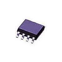
ORDERING INFORMATION
* Contact factory for industrial temperature range
GENERAL DESCRIPTION
The ALD1704 is a CMOS monolithic operational amplifier with MOSFET
input that has rail-to-rail input and output voltage ranges. The input voltage
range and output voltage range are very close to the positive and negative
power supply voltages. Typically the input voltage can be beyond positive
power supply voltage V
300mV. The output voltage swings to within 60mV of either positive or
negative power supply voltages at rated load.
This device is designed as an alternative to the popular JFET input
operational amplifiers in applications where lower operating voltages, such
as 9V battery or 3.25V to 6V power supplies are being used. It offers high
slew rate of 5V/ s at low operating power of 30mW. Since the ALD1704
is designed and manufactured with Advanced Linear Devices' standard
enhanced ACMOS silicon gate CMOS process, it also offers low unit cost
and exceptional reliability.
The rail-to-rail input and output feature of the ALD1704 allows a lower
operating supply voltage for a given signal voltage range and allows
numerous analog serial stages to be implemented without losing
operating voltage margin. The output stage is designed to drive up to 10mA
into 400pF capacitive and 1.5K
4000 pF at a gain of 5. Short circuit protection to either ground or the power
supply rails is at approximately 15mA clamp current. Due to complemen-
tary output stage design, the output can both source and sink 10mA into
a load with symmetrical drive and is ideally suited for applications where
push-pull voltage drive is desired.
The offset voltage is trimmed on-chip to eliminate the need for external
nulling in many applications. For precision applications, the output is
designed to settle to 0.1% in 2 s. For large signal buffer applications, the
operational amplifier can function as an ultra high input impedance voltage
follower/buffer that allows input and output voltage swings from positive to
negative supply voltages. This feature is intended to greatly simplify
systems design and eliminate higher voltage power supplies in many
applications.
© 1998 Advanced Linear Devices, Inc. 415 Tasman Drive, Sunnyvale, California 94089 -1706 Tel: (408) 747-1155 Fax: (408) 747-1286 http://www.aldinc.com
-55 C to +125 C
8-Pin
CERDIP
Package
ALD1704A DA
ALD1704B DA
ALD1704 DA
ALD1704G DA
A
L
D
INEAR
DVANCED
EVICES,
Operating Temperature Range
+
I
, or the negative power supply voltage V- by up to
NC.
0 C to +70 C
8-Pin
Small Outline
Package (SOIC)
ALD1704A SA
ALD1704B SA
ALD1704 SA
ALD1704G SA
RAIL-TO-RAIL CMOS OPERATIONAL AMPLIFIER
resistive loads at unity gain and up to
0 C to +70 C
8-Pin
Plastic Dip
Package
ALD1704A PA
ALD1704B PA
ALD1704 PA
ALD1704G PA
• Output settles to 2mV of supply rails
• High capacitive load capability -- up to 4000pF
• Symmetrical push-pull output drives
• No frequency compensation required --
• Extremely low input bias currents -- 1.0pA
• Ideal for high source impedance applications
• High voltage gain -- typically 150V/mV
• Output short circuit protected
• Unity gain bandwidth of 2.1MHz
FEATURES
• Rail-to-rail input and output voltage ranges
• 5.0V/ s slew rate
APPLICATIONS
• Voltage amplifier
• Voltage follower/buffer
• Charge integrator
• Photodiode amplifier
• Data acquisition systems
• High performance portable
• Signal conditioning circuits
• Low leakage amplifiers
• Active filters
• Sample/Hold amplifier
• Picoammeter
• Current to voltage converter
• Coaxial cable driver
• Capacitive sensor amplifier
• Piezoelectric transducer amplifier
PIN CONFIGURATION
unity gain stable
typical (20pAMax)
instruments
N/C
+IN
-IN
V -
* N/C Pin is internally connected. Do not connect externally.
2
3
4
1
DA, PA, SA PACKAGE
ALD1704A/ALD1704B
TOP VIEW
ALD1704/ALD1704G
8
6
5
7
N/C
V +
OUT
N/C


