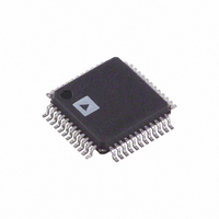
ADV7173KSTZ Analog Devices Inc, ADV7173KSTZ Datasheet - Page 30

ADV7173KSTZ
Manufacturer Part Number
ADV7173KSTZ
Description
IC DAC VIDEO NTSC 6-CH 48LQFP
Manufacturer
Analog Devices Inc
Type
Video Encoderr
Datasheet
1.ADV7173KSTZ.pdf
(60 pages)
Specifications of ADV7173KSTZ
Applications
Multimedia
Voltage - Supply, Analog
4.75 V ~ 5.25 V
Mounting Type
Surface Mount
Package / Case
48-LQFP
Input Format
Digital
Output Format
Analog
Supply Voltage Range
3V To 3.6V
Operating Temperature Range
0°C To +70°C
Tv / Video Case Style
LQFP
No. Of Pins
48
Msl
MSL 1 - Unlimited
Lead Free Status / RoHS Status
Lead free / RoHS Compliant
For Use With
EVAL-ADV7173EBM - BOARD EVAL FOR ADV7173
Voltage - Supply, Digital
-
Lead Free Status / RoHS Status
Lead free / RoHS Compliant, Lead free / RoHS Compliant
Available stocks
Company
Part Number
Manufacturer
Quantity
Price
Company:
Part Number:
ADV7173KSTZ
Manufacturer:
ADI
Quantity:
1 135
Company:
Part Number:
ADV7173KSTZ
Manufacturer:
Analog Devices Inc
Quantity:
10 000
Part Number:
ADV7173KSTZ
Manufacturer:
ADI/亚德诺
Quantity:
20 000
Company:
Part Number:
ADV7173KSTZ-REEL
Manufacturer:
ADI
Quantity:
7 101
Company:
Part Number:
ADV7173KSTZ-REEL
Manufacturer:
Analog Devices Inc
Quantity:
10 000
ADV7172/ADV7173
MODE REGISTER 4 MR4 (MR47–MR40)
(Address (SR4–SR0) = 04H)
Mode Register 4 is a 8-bit wide register. Figure 48 shows the
various operations under the control of Mode Register 4.
MR4 BIT DESCRIPTION
VSYNC_3H (MR40)
When this bit is enabled (“1”) in slave mode, it is possible to
drive the VSYNC active low input for 2.5 lines in PAL mode
and 3 lines in NTSC mode. When this bit is enabled in master
mode, the ADV7172/ADV7173 outputs an active low VSYNC
signal for 3 lines in NTSC mode and 2.5 lines in PAL mode.
Genlock Selection (MR42–MR41)
These bits control the genlock feature of the ADV7172/ADV7173.
Setting MR41 to Logic “0” disables the SCRESET/RTC pin
and allows the ADV7172/ADV7173 to operate in normal mode.
By setting MR41 to “1,” one of two operations may be enabled:
1. If MR42 is set to “0,” the SCRESET/RTC pin is configured
2. If MR42 is set to “1,” the SCRESET/RTC pin is configured
as a subcarrier reset input and the subcarrier phase will reset
to Field 0 whenever a low-to-high field transition is detected
on the SCRESET/RTC pin.
as a real-time control input and the ADV7172/ADV7173 can
be used to lock to an external video source.
MR47
0
1
MODE CONTROL
INTERLACED
INTERLACED
NONINTERLACED
MR47
MR46
COLOR BAR
0
1
CONTROL
DISABLE
ENABLE
MR46
MR45
0
1
CONTROL
ENABLE BURST
DISABLE BURST
BURST
MR45
MR44
0
1
CHROMINANCE
ENABLE COLOR
DISABLE COLOR
CONTROL
MR44
MR43
0
1
Active Video Line Duration (MR43)
This bit switches between two active video line durations. A
“0” selects CCIR REC 601 (720 pixels PAL/NTSC) and a “1”
selects ITU-R.BT 470 “analog” standard for active video dura-
tion (710 pixels NTSC, 702 pixels PAL).
Chrominance Control (MR44)
This bit enables the color information to be switched on and off
the video output.
Burst Control (MR45)
This bit enables the color burst information to be switched on
and off the video output.
Color Bar Control (MR46)
This bit can be used to generate and output an internal color
bar test pattern. The color bar configuration is 100/7.5/75/7.5
for NTSC and 100/0/75/0 for PAL. It is important to note that
when color bars are enabled, the ADV7172/ADV7173 is config-
ured in a master timing mode. The output pins VSYNC/FIELD,
HSYNC and BLANK are three-state during color bar mode.
Interlaced Mode Control (MR47)
This bit is used to set up the output to interlaced or noninter-
laced mode.
LINE DURATION
ACTIVE VIDEO
MR43
720 PIXELS
710/702 PIXELS
MR42 MR41
x
0
1
GENLOCK SELECTION
MR42
0
1
1
DISABLE GENLOCK
ENABLE SUBCARRIER
RESET PIN
ENABLE RTC PIN
MR41
MR40
MR40
0
1
VSYNC 3H
DISABLE
ENABLE


