BU1425AKV Rohm Semiconductor, BU1425AKV Datasheet - Page 14
BU1425AKV
Manufacturer Part Number
BU1425AKV
Description
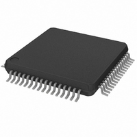
IC ENCODER NTSC/PAL DGTL VQFP64
Manufacturer
Rohm Semiconductor
Type
NTSC/PAL Encoderr
Datasheet
1.BU1425AK.pdf
(33 pages)
Specifications of BU1425AKV
Applications
Video
Voltage - Supply, Analog
4.5 V ~ 5.5 V
Voltage - Supply, Digital
4.5 V ~ 5.5 V
Mounting Type
Surface Mount
Package / Case
64-TQFP, 64-VQFP
Lead Free Status / RoHS Status
Lead free / RoHS Compliant
Available stocks
Company
Part Number
Manufacturer
Quantity
Price
Company:

Part Number:
BU1425AKV
Manufacturer:
Rohm Semiconductor
Quantity:
10 000


Also, setting the CLKSW pin to HIGH enables the fre-
quency of the external clock to be used as BCLK, the
internal clock, just as it is. Since the data is read to the
With the BU1425AK / AKV, the sub-carrier (burst) fre-
quency is generated using the internal clock. For this
reason, the frequencies used in the various modes are
Table 7: BU1425AK / AKV clock input frequency settings
The BU1425AK / AKV has an "Encoder Master" mode in
which synchronization signals are output, and an
"Encoder Slave" mode in which synchronization signals
are input from an external source and used to achieve
synchronization. These modes are switched at the
SLABEB pin. When the SLABEB pin is LOW, the Slave
mode is in effect, and when HIGH, the Master mode is in
effect.
In the Master mode, the HSY and VSY pins serve as out-
put, with horizontal synchronization signals (HSYNC)
being output from the HSY pin and vertical synchroniza-
tion signals (VSYNC) from the VSY pin. At this time, the
reference timing for synchronization signal output is
determined at the rising edge of the RSTB pin. Output is
obtained in accordance with the specified mode (NTSC,
PAL, or PAL60, interlace or non-interlace). Output in the
14
5) Synchronization signals
Multimedia ICs
CLKSW Pin
0
1
HSY
VCLK
Internal clock (BCLK)
Input data
Same for NTSC / PAL / PAL60
Video-CD Mode
Fig. 4 Illustration of clock timing (CLKSW is HIGH)
27.000MHz
13.500MHz
BU1425AK / AKV at the rising edge of BCLK at this
time as well, data should be input as shown in Fig. 4.
The relationship with HSY is also as shown in Fig. 4.
limited, so those frequencies should be input (see Table
7 below).
non-interlace mode, however, is output only under "Odd"
field conditions (the falling edges of Hsy and Vsy are the
same).
In the Slave mode, the HSY and VSY pins serve as input,
and horizontal synchronization signals (HSYNC) should
be input to the HSY pin and vertical synchronization sig-
nals (VSYNC) to the VSY pin. The input synchronization
signals at this time should be input in accordance with
the specified mode. With the BU1425AK / AKV, field dis-
tinction between odd and even fields is made automati-
cally for each field when interlace input is used. With the
BU1425AK, all synchronization signals are treated as
negative polarity signals (signals for which the sync inter-
val goes LOW). When using the non-interlace mode,
operation is normally carried out under odd field condi-
tions (the falling edges of Hsy and Vsy are simultane-
ous).
28.636MHz
14.318MHz
NTSC
BU1425AK / BU1425AKV
CD-G Mode
PAL / PAL60
28.3750MHz
14.1875MHz
Related parts for BU1425AKV
Image
Part Number
Description
Manufacturer
Datasheet
Request
R

Part Number:
Description:
Manufacturer:
Rohm Semiconductor
Datasheet:
Part Number:
Description:
Manufacturer:
Rohm Semiconductor
Datasheet:
Part Number:
Description:
Manufacturer:
Rohm Semiconductor
Datasheet:
Part Number:
Description:
Manufacturer:
Rohm Semiconductor
Datasheet:
Part Number:
Description:
Manufacturer:
Rohm Semiconductor
Datasheet:
Part Number:
Description:
Manufacturer:
Rohm Semiconductor
Datasheet:
Part Number:
Description:
Manufacturer:
Rohm Semiconductor
Datasheet:
Part Number:
Description:
Manufacturer:
Rohm Semiconductor
Datasheet:
Part Number:
Description:
Manufacturer:
Rohm Semiconductor
Datasheet:
Part Number:
Description:
Manufacturer:
Rohm Semiconductor
Datasheet:
Part Number:
Description:
Manufacturer:
Rohm Semiconductor
Datasheet:
Part Number:
Description:
Manufacturer:
Rohm Semiconductor
Datasheet:

Part Number:
Description:
DIODE SWITCH 80V 25MA SMD5 TR
Manufacturer:
Rohm Semiconductor
Datasheet: