AD1893JN Analog Devices Inc, AD1893JN Datasheet
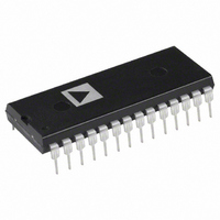
IC SAMPLE-RATE CONV 16BIT 28DIP

AD1893JN

Manufacturer Part Number
AD1893JN
Description
IC SAMPLE-RATE CONV 16BIT 28DIP
Manufacturer
Analog Devices Inc
Series
SamplePort™r
Type
Sample Rate Converterr
Datasheet

Specifications of AD1893JN

Rohs Status
RoHS non-compliant
Applications
Multimedia
Voltage - Supply, Digital
2.7 V ~ 5.5 V
Mounting Type
Through Hole
Package / Case
28-DIP (0.600", 15.24mm)
Voltage - Supply, Analog
-
a
PRODUCT OVERVIEW
The AD1893 SamplePort is a fully digital, stereo Asynchronous
Sample Rate Converter (ASRC) that solves sample rate interfacing
and compatibility problems in digital audio equipment. Concep-
tually, this converter interpolates the input data up to a very high
internal sample rate with a time resolution of 300 ps, then deci-
mates down to the desired output sample rate. The AD1893 is
intended for 16-bit low cost, non-varispeed applications where low
voltage, low power (i.e., battery-powered) operation is required.
Refer to the AD1890/AD1891 data sheet for other products in the
SamplePort family. This device is asynchronous because the fre-
quency and phase relationships between the input and output
sample clocks (both are inputs to the AD1893 ASRC) are arbitrary
and need not be related by a simple integer ratio. There is no need
to explicitly select or program the input and output sample clock
frequencies, as the AD1893 automatically senses the relationship
between the two clocks. The input and output sample clock fre-
quencies can nominally range from 8 kHz to 56 kHz, and the ratio
between them can vary from approximately 1:2 to 2:1.
SamplePort is a registered trademark of Analog Devices, Inc.
REV. A
Information furnished by Analog Devices is believed to be accurate and
reliable. However, no responsibility is assumed by Analog Devices for its
use, nor for any infringements of patents or other rights of third parties
which may result from its use. No license is granted by implication or
otherwise under any patent or patent rights of Analog Devices.
FEATURES
Low Cost
LQFP and PDIP Packages
3 V Supply Performance Specified—Very Low Power
Automatically Senses Sample Frequencies—No
Rejects Sample Clock Jitter
Accommodates Dynamically Changing Asynchronous
8 kHz to 56 kHz Sample Clock Frequency Range
Approximately 1:2 to 2:1 Ratio Between Sample
–96 dB THD+N at 1 kHz
96 dB Dynamic Range
Optimal Clock Tracking Control—Slow/Fast Settling
Linear Phase in All Modes
Automatic Output Mute
Flexible Four-Wire Serial Interfaces with Right-Justified
Power-Down Mode
On-Chip Oscillator
APPLICATIONS
Consumer CD-R, DAT, DCC, MD and 8 mm Video Tape
Digital Audio Communication/Network Systems
Computer Multimedia Systems
Programming Required
Sample Clocks
Clocks
Mode
Recorders Including Portables
Modes
The AD1893 uses multirate digital signal processing techniques
to construct an output sample stream from the input sample
stream. The input word width is 4 to 16 bits for the AD1893.
Shorter input words are automatically zero-filled in the LSBs.
The output word width is 24 bits. The user can receive as many
of the output bits as desired. Internal arithmetic is performed
with 22-bit coefficients and 27-bit accumulation. The digital
samples are processed with unity gain.
The input and output control signals allow for considerable
flexibility for interfacing to a variety of DSP chips, AES/EBU
receivers and transmitters and for I
and output data can be independently right- or left- (with or
without a one bit clock delay) justified to the left/right clock
edge. In the right-justified mode, the MSB is delayed 16-bit
clock periods from the left/right clock edge transition. Input and
output data can also be independently justified to the word
clock rising edge. The data justification options are encoded on
two mode pins for both the input port and the output port. The
bit clocks can also be independently configured for rising edge
active or falling edge active operation.
The AD1893 SamplePort ASRC has on-chip digital coefficients
that correspond to a highly oversampled 0 Hz to 20 kHz low-
pass filter with a flat passband, a very narrow transition band,
and a high degree of stopband attenuation. A subset of these
filter coefficients are dynamically chosen on the basis of the
filtered ratio between the input sample clock (LR_I) and the
output sample clock (LR_O), and these coefficients are then
used in an FIR convolver to perform the sample rate conversion.
Refer to the Theory of Operation section of this data sheet for a
more thorough functional description. The low-pass filter has
been designed so that full 20 kHz bandwidth is maintained
when the input and output sample clock frequencies are as low
as 44.1 kHz. If the output sample rate drops below the input
sample rate, the bandwidth of the input signal is automatically
One Technology Way, P.O. Box 9106, Norwood, MA 02062-9106, U.S.A.
Tel: 781/329-4700
Fax: 781/326-8703
INPUT SAMPLE CLOCK
BROADCAST 32kHz
INPUT SERIAL DATA
FREQUENCIES:
CD 44.1kHz OR
DAT 48kHz OR
EXAMPLE
16-Bit Stereo Asynchronous
Sample Rate Converter
Low Cost SamplePort
SYSTEM DIAGRAM
World Wide Web Site: http://www.analog.com
AD1893
2
S compatible devices. Input
© Analog Devices, Inc., 1998
OUTPUT SAMPLE CLOCK
OUTPUT SERIAL DATA
(continued on Page 4)
AD1893
BROADCAST 32kHz
FREQUENCIES:
CD 44.1kHz OR
DAT 48kHz OR
EXAMPLE
®

Related parts for AD1893JN

AD1893JN Summary of contents

Page 1

FEATURES Low Cost LQFP and PDIP Packages 3 V Supply Performance Specified—Very Low Power Automatically Senses Sample Frequencies—No Programming Required Rejects Sample Clock Jitter Accommodates Dynamically Changing Asynchronous Sample Clocks 8 kHz to 56 kHz Sample Clock Frequency Range ...

Page 2

AD1893–SPECIFICATIONS TEST CONDITIONS UNLESS OTHERWISE NOTED Supply Voltage +3.0 Ambient Temperature 25 Crystal Frequency 16 Load Capacitance 100 All minimums and maximums tested except as noted. 1 PERFORMANCE (Guaranteed for V Dynamic Range ( kHz, –60 dB ...

Page 3

... Exposure to absolute maximum rating conditions for extended periods may affect device reliability. Specifications subject to change without notice. Model AD1893JN AD1893JST CAUTION ESD (electrostatic discharge) sensitive device. Electrostatic charges as high as 4000 V readily accumulate on the human body and test equipment and can discharge without detection ...

Page 4

AD1893 (continued from Page 1) PRODUCT OVERVIEW (Continued) limited to avoid alias distortion on the output signal. The AD1893 dynamically alters the low-pass filter cutoff frequency smoothly and slowly, so that real-time variations in the sample rate ratio are possible ...

Page 5

DIP XTAL_O 1 SERIAL IN 2 XTAL_I DATA_I 3 SERIAL OUT BCLK_I 4 WCLK_I 5 ACCUM 6 LR_I GND MULT NC 9 BKPOL_I 10 FIFO COEF ROM MODE0_I 11 12 MODE1_I RESET 13 CLOCK TRACKING GND ...

Page 6

AD1893 Output Control Signals Pin Name DIP LQFP I/O Description BKPOL_O Bit clock polarity. LO: Normal mode. Output data is valid on rising edges of BCLK_O, changed on falling. HI: Inverted mode. Output data is valid on ...

Page 7

THEORY OF OPERATION There are at least two logically equivalent methods of explaining the concept of asynchronous sample rate conversion: the high speed interpolation/decimation model and the polyphase filter bank model. Using the AD1893 SamplePort does not require understanding either ...

Page 8

AD1893 Polyphase Filter Bank Model Although less intuitively understandable than the interpolation/ decimation model, the polyphase filter bank model is useful to explore because it more accurately portrays the operation of the actual AD1893 SamplePort hardware. In the polyphase filter ...

Page 9

AMP Figure 3. Four Polyphase Subfilters Realigned to Coarse Time Grid POLYPHASE FILTER 1 POLYPHASE FILTER 2 POLYPHASE FILTER 3 POLYPHASE FILTER 4 POLYPHASE FILTER 5 POLYPHASE FILTER 6 INPUT POLYPHASE FILTER 7 SIGNAL POLYPHASE FILTER N-1 POLYPHASE FILTER N ...

Page 10

AD1893 OFFSET INTO DENSE FIR FILTER COEFFICIENT ARRAY TO ACCESS REQUIRED POLYPHASE FILTER REQUIRED FILTER GROUP DELAY TO COMPUTE REQUESTED OUTPUT SAMPLE A INPUT SEQUENCE PAST OUTPUT SEQUENCE Figure 5. Input and Output Clock Event Relationship A short delay corresponds ...

Page 11

Sample Clock Jitter Rejection The loop filter settling time also affects the ability of the AD1893 ASRC to reject sample clock jitter, since the control loop effectively computes a time weighted average or “esti- mated” new output of many past ...

Page 12

AD1893 Cutoff Frequency Modification The final important operating concept of the ASRC is the modi- fication of the filter cutoff frequency when the output sample rate (F ) drops below the input sample rate (F SOUT during downsampling operation. The ...

Page 13

OPERATING FEATURES Serial Input/Output Ports The AD1893 uses the frequency of the left/right input clock (LR_ I) and the left/right output clock (LR_O) signals to deter- mine the sample rate ratio, and therefore these signals must run continuously and transition ...

Page 14

AD1893 Some applications using multiple AD1893s may desire to use the same master clock frequency for all the SamplePorts, sup- plied by a single crystal. The crystal output can be buffered with a 74HCXX gate and distributed to the other ...

Page 15

1/2 6kHz SIN SOUT UP- 42kHz SAMPLING 32 DOWN- 24 SAMPLING 16 42kHz – kHz SIN Figure 12. Allowable Input ...

Page 16

AD1893 System Mute The mute function applies to both right and left channels on the AD1893. The user can include a system-specific output mute signal, while retaining the automatic mute feature of the AD1893 by using the circuit shown in ...

Page 17

AMPLITUDE – dBFS Figure 19. THD+N vs. Input Amplitude, 44.1 kHz Input Sample Frequency, 48 kHz Output Sample Frequency, 1 kHz and ...

Page 18

AD1893 BCLK_I, BCLK_O NORMAL MODE INPUT BCLK_I, BCLK_O INVERTED MODE LR_I, LR_O INPUT WCLK_I, WCLK_O INPUT DATA IN/OUT Figure 23. Serial Data Input and Output Timing, Word Clock Triggered Mode BCLK_I, BCLK_O NORMAL MODE INPUT BCLK_I, BCLK_O INVERTED MODE LR_I, ...

Page 19

CRYSTAL t CRYSTAL Figure 26. Clock Timing BCLK_I, BCLK_O BCLK_I, BCLK_O INVERTED MODE NO MSB DELAY MODE NO MSB DELAY MODE MSB DELAY MODE MSB DELAY MODE Figure 28. Bit Clock, Word Clock, Left / Right Clock and Data Timing ...

Page 20

AD1893 0.250 (6.35) MAX 0.200 (5.05) 0.125 (3.18) OUTLINE DIMENSIONS Dimensions shown in inches and (mm). 28-Lead Plastic DIP (N-28) 1.565 (39.70) 1.380 (35.10 0.580 (14.73) 0.485 (12.32 0.625 (15.87) PIN 1 0.060 (1.52) 0.600 (15.24) ...

Related keywords