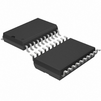
LTC1060CSW#TR Linear Technology, LTC1060CSW#TR Datasheet - Page 16

LTC1060CSW#TR
Manufacturer Part Number
LTC1060CSW#TR
Description
IC BUILDING BLK DUAL FLTR 20SOIC
Manufacturer
Linear Technology
Datasheet
1.LTC1060CNPBF.pdf
(20 pages)
Specifications of LTC1060CSW#TR
Filter Type
Universal Switched Capacitor
Frequency - Cutoff Or Center
30kHz
Number Of Filters
2
Max-order
4th
Voltage - Supply
±2.37 V ~ 5 V
Mounting Type
Surface Mount
Package / Case
20-SOIC (7.5mm Width)
Architecture
Switched Capacitor
Cutoff Frequency
20KHz
Single Supply Voltage (typ)
5V
Dual Supply Voltage (typ)
±5V
Power Supply Requirement
Single/Dual
Single Supply Voltage (min)
4.74V
Single Supply Voltage (max)
16V
Dual Supply Voltage (min)
±2.37V
Dual Supply Voltage (max)
±8V
Operating Temperature (min)
-40C
Operating Temperature (max)
85C
Package Type
SOIC W
Lead Free Status / RoHS Status
Contains lead / RoHS non-compliant
Available stocks
Company
Part Number
Manufacturer
Quantity
Price
COMM
In mode 3 (Figure 11), a single resistor ratio (R2/R4) can
tune the center frequency below or above the f
(or f
since it provides a highpass, bandpass, lowpass output
through progressive integration; notches are obtained by
summing the highpass and lowpass outputs (mode 3a,
Figure 12). The notch frequency can be tuned below or
above the center frequency through the resistor ratio
(R
versatile and useful modes for cascading second order
sections to obtain high order elliptic filters. Figure 20
shows the two sections of an LTC1060 connected in mode
3a to obtain a clock tunable 4th order sharp elliptic
bandpass filter. The first notch is created by summing
directly the HP and LP outputs of the first section into the
inverting input of the second section op amp. The indi-
vidual Q’s are 29.6 and the filter maintains its shape and
performance up to 20kHz center frequency (Figure 21).
For this circuit an external op amp is required to obtain the
2nd notch. The dynamics of Figure 20 are excellent be-
LTC1060
Modes 2, 2a, and 2b have a notch output which frequency,
f
f
when cascading second order functions to create an
16
n
0
, can be tuned independently from the center frequency,
. For all cases, however, f
T
h
V
2
IN
/R
L OR CMOS CLK IN
CLK
W W
R61
i
). Because of this, modes 3 and 3a are the most
R11
Figure 19. Cascading the Two Sections of the LTC1060 Connected in Mode 1c to Obtain a Clock Tunable 4th Order
1dB Ripple Bandpass Chebyshev Filter with (Center Frequency)/(Ripple Bw) = 20/1.
/50) ratio. Mode 3 is a state variable configuration
V + = 5V
E TS
U
R51
R31
R21
R11 = 149.21k
R21 = 4.99k
R31 = 149.12k
R51 = 2.55k
R61 = 2.49k
PRECISE RESISTOR VALUES
10
1
2
3
4
5
6
7
8
9
ON
LP
BP
N
INV
S1A
S
V
V
LSh
CLK
A
A/B
A
D
A
+
A
+
A
U
LTC1060
A
n
THE
50/100
<f
AGND
CLK
INV
BP
S1B
R12 = 45.14k
R22 = 5.00k
R32 = 142.64k
R5 = 2.49k
R62 = 4.29k
LP
V
V
0
N
D
A
. These modes are useful
B
B
B
B
B
–
–
20
19
18
17
16
15
14
13
12
11
M
W
5V
R52
R32
R22
V
ODES OF OPERATIO
–
= –5V
R62
CLK
LTC1060 • CM01
R12
/100
V
OUT
overall elliptic highpass, bandpass or notch response. The
input amplifier and its feedback resistors (R2/R4) are now
part of the resonant loop. Because of this, mode 2 and its
derivatives are slower than mode 1’s.
cause the amplitude response at each output pin does not
exceed 0dB. The gain in the passband depends on the ratio
of (R
obtained by acting on the (R
amp, meanwhile the remaining ratios are adjusted for
optimum dynamics of the LTC1060 output nodes. The
external op amp of Figure 20 is not always required. In
Figure 22, one section of the LTC1060 in mode 3a is
cascaded with the other section in mode 2b to obtain a 4th
order, 1dB ripple, elliptic bandreject filter. This configura-
tion is interesting because a 4th order function with two
different notches is realized without requiring an external
op amp. The clock-to-center frequency ratio is adjusted to
200:1; this is done in order to better approximate a linear
R,C notch filter. The amplitude response of the filter is
shown in Figure 23 with up to 1MHz clock frequency. The
0dB bandwidth to the stop bandwidth ratio is 9/1. When
the filter is centered at 1kHz, it should theoretically have a
44dB rejection with a 50Hz stop bandwidth. For a more
narrow filter than the above, the unused BP output of the
g
/R
–10dB
–15dB
–20dB
–25dB
–10dB
–15dB
–20dB
–25dB
–5dB
–5dB
0dB
0dB
h2
0.9kHz
18kHz
) • (R22/R
U
19kHz
h1
)• (R21/R11). Any gain value can be
20kHz
50Hz
1kHz
1kHz
g
/R
21kHz
h2
) ratio of the external op
f
f
CLK
1.1kHz
CLK
22kHz
TLC1060 • CMO01b
= 800kHz
= 40kHz
1060fb


