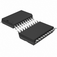
LTC1060CSW#TR Linear Technology, LTC1060CSW#TR Datasheet - Page 7

LTC1060CSW#TR
Manufacturer Part Number
LTC1060CSW#TR
Description
IC BUILDING BLK DUAL FLTR 20SOIC
Manufacturer
Linear Technology
Datasheet
1.LTC1060CNPBF.pdf
(20 pages)
Specifications of LTC1060CSW#TR
Filter Type
Universal Switched Capacitor
Frequency - Cutoff Or Center
30kHz
Number Of Filters
2
Max-order
4th
Voltage - Supply
±2.37 V ~ 5 V
Mounting Type
Surface Mount
Package / Case
20-SOIC (7.5mm Width)
Architecture
Switched Capacitor
Cutoff Frequency
20KHz
Single Supply Voltage (typ)
5V
Dual Supply Voltage (typ)
±5V
Power Supply Requirement
Single/Dual
Single Supply Voltage (min)
4.74V
Single Supply Voltage (max)
16V
Dual Supply Voltage (min)
±2.37V
Dual Supply Voltage (max)
±8V
Operating Temperature (min)
-40C
Operating Temperature (max)
85C
Package Type
SOIC W
Lead Free Status / RoHS Status
Contains lead / RoHS non-compliant
Available stocks
Company
Part Number
Manufacturer
Quantity
Price
Power Supplies
The V
(Pins 14 and 13) are, respectively, the analog and digital
positive and negative supply pins. For most cases, Pins 7
and 8 should be tied together and bypassed by a 0.1µF disc
ceramic capacitor. The same holds for Pins 13 and 14. If
the LTC1060 operates in a high digital noise environment,
the supply pins can be bypassed separately. Pins 7 and 8
are internally connected through the IC substrate and
should be biased from the same DC source. Pins 13 and
14 should also be biased from the same DC source.
The LTC1060 is designed to operate with ±2.5V supply
(or single 5V) and with ± 5V to ±8V supplies. The mini-
mum supply, where the filter operates reliably, is ± 2.37V.
With low supply operation, the maximum input clock
frequency is about 500kHz. Beyond this, the device exhib-
its excessive Q enhancement and center frequency errors.
Clock Input Pins and Level Shift
The level shift (LSh) Pin 9 is used to accommodate T
CMOS clock levels. With dual supplies equal or higher
to ±4.5V, Pin 9 should be connected to ground (same
potential as the AGND pin). Under these conditions the
clock levels can be T
operation, the negative supply pins and the LSh pin should
be tied to the system ground. The AGND, Pin 15, should
be biased at 1/2 supplies, as shown in the “Single 5V Gain
of 1000 4th Order Bandpass Filter” circuit. Again, under
these conditions, the clock levels can be T
input clock pins (10,11) share the same level shift pin.
The clock logic threshold level over temperature is
typically 1.5V ± 0.1V above the LSh pin potential. The duty
cycle of the input clock should be close to 50%. For clock
frequencies below 1MHz, the (f
from the clock input levels and from its rise and fall times.
Fast rising clock edges, however, improve the filter DC
offsets. For clock frequencies above 1MHz, T
clocks are recommended.
50/100/Hold (Pin 12)
By tying Pin 12 to (V
50:1 mode. With ±5V supplies, Pin 12 can be typically 1V
below the positive supply without affecting the 50:1
PIN DESCRIPTION
U
+
A
and V
+
D
(pins 7 and 8) and the V
+
A
2
and V
L or CMOS. With single supply
U
+
D
CLK
AND APPLICATIONS INFORMATIO
), the filter operates in the
U
/f
0
) ratio is independent
2
L or CMOS. The
–
A
and V
2
L level
2
L or
–
D
U
operation of the device. By tying Pin 12 to 1/2 supplies
(which should be the AGND potential), the LTC1060
operates in the 100:1 mode. The 1/2 supply bias of Pin 12
can vary around the 1/2 supply potential without affecting
the 100:1 filter operation. This is shown in Table 1.
When Pin 12 is shorted to the negative supply pin, the filter
operation is stopped and the bandpass and lowpass
outputs act as a S/H circuit holding the last sample. The
hold step is 20mV and the droop rate is 150µV/second!
Table 1
S1
These are voltage signal input pins and, if used, they
should be driven with a source impedance below 5kΩ. The
S1
frequency ratio (f
2b) or to feedforward the input signal for allpass filter
configurations (see Modes 4 and 5). When these pins are
not used, they should be tied to the AGND pin.
S
When S
summer (see Block Diagram) is tied to the lowpass output.
This frees the S1 pin to realize various modes of operation
for improved applications flexibility. When the S
connected to the negative supply, the S2 input switches to
ground and internally becomes inactive. This improves
the filter noise performance and typically lowers the value
of the offset V
AGND (Pln 15)
This should be connected to the system ground for dual
supply operation. When the LTC1060 operates with a
single positive supply, the analog ground pin should be
tied to 1/2 supply and bypassed with a 0.1µF capacitor, as
shown in the application, “Single 5V, Gain of 1000 4th
Order Bandpass Filter.” The positive inputs of all the
A/B
A
A
, S1
, S1
U
TOTAL POWER SUPPLY
(Pin 6)
B
B
A/B
(Pins 5 and 16)
pins can be used to alter the CLK to center
is high, the S2 input of the filter’s voltage
10V
15V
5V
OS2
W
CLK
.
/f
0
) of the filter (see Modes 1b, 1c, 2a,
U
VOLTAGE RANGE OF PIN 12
FOR 100:1 OPERATION
7.5V ± 1.5V
2.5 ± 0.5V
LTC1060
5V ± 1V
A/B
pin is
1060fb
7


