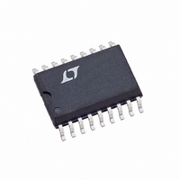
LTC1066-1CSW#TR Linear Technology, LTC1066-1CSW#TR Datasheet - Page 12

LTC1066-1CSW#TR
Manufacturer Part Number
LTC1066-1CSW#TR
Description
IC FILTER LP 8TH ORDER 18SOIC
Manufacturer
Linear Technology
Datasheet
1.LTC1066-1CSWPBF.pdf
(20 pages)
Specifications of LTC1066-1CSW#TR
Filter Type
Bessel, Lowpass Switched Capacitor
Frequency - Cutoff Or Center
50kHz
Number Of Filters
1
Max-order
8th
Voltage - Supply
4.75 V ~ 16 V, ±2.375 V ~ 8 V
Mounting Type
Surface Mount
Package / Case
18-SOIC (7.5mm Width)
Lead Free Status / RoHS Status
Contains lead / RoHS non-compliant
Available stocks
Company
Part Number
Manufacturer
Quantity
Price
LTC1066-1
APPLICATIONS
Transient Response and Settling Time
The LTC1066-1 exhibits two different transient behaviors.
First, during power-up the DC correcting loop will settle
after the voltage offset of the internal switched-capacitor
network is stored across the feedback capacitor C
Block Diagram). It takes approximately five time constants
(5R
settling, the filter reaches steady state. The filter transient
response is then defined by the frequency characteristics
of the internal switched-capacitor lowpass filter. Figure 5
shows details.
DC loop settling is also observed if, at steady state, the DC
offset of the internal switched-capacitor network suddenly
changes. A sudden change may occur if the clock fre-
quency is instantaneously stepped to a value above 1MHz.
12
Clock Feedthrough
Clock feedthrough is defined as the RMS value of the clock
frequency and its harmonics that are present at the filter’s
output pin (9). The clock feedthrough is tested with the
input pin (2) grounded and depends on PC board layout
F
C
F
INPUT
) for settling to 1%. Second, following DC loop
RISE TIME (t
SETTLING TIME (t
DELAY TIME (t
90%
10%
50%
Figure 5. Transient Response
r
)
d
)
U
s
t d
)
50:1 ELLIPTIC
t s
f
f
f
INFORMATION
CUTOFF
CUTOFF
CUTOFF
0.709
0.43
3.4
U
t r
±5%
±5%
±5%
100:1 LINEAR PHASE
W
f
f
f
CUTOFF
CUTOFF
CUTOFF
0.556
0.43
2.05
±5%
±5%
±5%
1066-1 F05
U
OUTPUT
F
(see
and on the value of the power supplies. With proper layout
techniques the values of the clock feedthrough are shown
on Table 7.
Table 7. Clock Feedthrough
Wideband Noise
The wideband noise of the filter is the total RMS value of
the device’s noise spectral density and is used to deter-
mine the operating signal-to-noise ratio. Most of its fre-
quency contents lie within the filter passband and cannot
be reduced with post filtering. For instance, the LTC1066-
1 wideband noise at ±5V supply is 100µV
which have frequency contents from DC up to the filter’s
cutoff frequency. The total wideband noise (µV
nearly independent of the value of the clock. The clock
feedthrough specifications are not part of the wideband
noise. Table 8 lists the typical wideband noise for each
supply.
Table 8. Wideband Noise
Speed Limitations
To avoid op amp slew rate limiting at maximum clock
frequencies, the signal amplitude should be kept below a
specified level as shown in Table 9.
Table 9. Maximum V
POWER SUPPLY
POWER SUPPLY
INPUT FREQUENCY
Single 5V
±5V
±7.5V
Single 5V
±5V
±7.5V
≥250kHz
≥700kHz
IN
100µV
160µV
100µV
106µV
70µV
90µV
50:1
50:1
RMS
RMS
RMS
RMS
RMS
RMS
MAXIMUM V
0.50V
0.25V
100:1 (Pin 8 to GND)
RMS
RMS
RMS
200µV
650µV
IN
90µV
80µV
85µV
90µV
, 95µV
100:1
RMS
RMS
RMS
RMS
RMS
RMS
RMS
RMS
10661fa
) is
of


