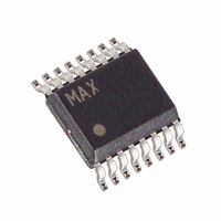
MAX7490CEE+T Maxim Integrated Products, MAX7490CEE+T Datasheet - Page 5

MAX7490CEE+T
Manufacturer Part Number
MAX7490CEE+T
Description
IC FILTER SW CAP DUAL 16-QSOP
Manufacturer
Maxim Integrated Products
Datasheet
1.MAX7490EEE.pdf
(18 pages)
Specifications of MAX7490CEE+T
Filter Type
Universal Switched Capacitor
Frequency - Cutoff Or Center
40kHz
Number Of Filters
2
Max-order
2nd
Voltage - Supply
4.5 V ~ 5.5 V
Mounting Type
Surface Mount
Package / Case
16-QSOP
Lead Free Status / RoHS Status
Lead free / RoHS Compliant
ELECTRICAL CHARACTERISTICS—MAX7491 (continued)
(V
GND; 50% duty-cycle clock input; COM = V
(Note 1)
Note 1: Resistive loading of the N_/HP_, LP_, BP_ outputs includes the resistors used for the filter implementation.
Note 2: Crosstalk between internal filter sections is measured by applying a 1V
Note 3: Bandwidth of noise measurement is 80kHz.
Note 4: f
(V
R2 = 10kΩ, Q = 5, T
POWER REQUIREMENTS
Supply Voltage
Power-Supply Current
Shutdown Current
Output Short-Circuit Current
DC Open-Loop Gain
Gain Bandwidth Product
Slew Rate
INTERNAL OP AMPS CHARACTERISTICS
DD
DD
-50
-10
-20
-30
-40
-60
= V
10
= +5V for MAX7490, V
0
1
and grounding the input of the other bandpass filter section. The crosstalk is the ratio between the output of the grounded
filter section and the 1V
EXTCLK
OSC
PARAMETER
2ND-ORDER BANDPASS FILTER
(kHz) = 135 x 10
FREQUENCY RESPONSE
Dual Universal Switched-Capacitor Filters
= +3V; f
FREQUENCY (kHz)
A
_______________________________________________________________________________________
= +25°C, unless otherwise noted.)
10
CLK
DD
3
= +3V for MAX7491, f
= 625kHz; 10kΩ || 50pF load to V
RMS
/ C
OSC
input signal of the other section.
SYMBOL
I
GBW
SHDN
V
(C
I
SR
100
DD
DD
OSC
DD
in pF)
/2; T
No load, mode 1, R1 = R3 = 50kΩ,
R2 = 10kΩ, Q = 5
SHDN = GND
R
R
R
300
250
200
150
100
50
L
L
L
0
CLK
≥ 10kΩ, C
≥ 10kΩ, C
≥ 10kΩ, C
A
1
V
f
Q = 5
CLK
= T
DD
= 625kHz, V
2ND-ORDER BANDPASS FILTER
= +5V
= 625kHz
MIN
L
L
L
PHASE RESPONSE
to T
CONDITIONS
≤ 50pF
≤ 50pF
≤ 50pF
FREQUENCY (kHz)
DD
MAX
SHDN
/2 at LP_, BP_, and N_/HP_; V
10
. Typical values are at T
Typical Operating Characteristics
= V
EXTCLK
RMS
10kHz signal to one bandpass filter section input
= V
100
DD
, COM = V
-0.7
-0.1
-0.2
-0.3
-0.4
-0.5
-0.6
-0.8
0
A
100
MIN
2.7
= +25°C, unless otherwise noted.)
SHDN
DEVIATION vs. CLOCK FREQUENCY
CLOCK-TO-CENTER FREQUENCY
DD
/2, Mode 1, R3 = R1 = 50kΩ,
= V
TYP
±11
130
3.5
7
6
DD
V
f
DD
CLK
; 0.1µF from COM to
1000
= 5V
V
(kHz)
DD
MAX
= 3V
3.6
4.0
1
UNITS
MHz
V/μs
mA
mA
μA
dB
V
10,000
5


