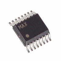
MAX7490CEE+T Maxim Integrated Products, MAX7490CEE+T Datasheet - Page 8

MAX7490CEE+T
Manufacturer Part Number
MAX7490CEE+T
Description
IC FILTER SW CAP DUAL 16-QSOP
Manufacturer
Maxim Integrated Products
Datasheet
1.MAX7490EEE.pdf
(18 pages)
Specifications of MAX7490CEE+T
Filter Type
Universal Switched Capacitor
Frequency - Cutoff Or Center
40kHz
Number Of Filters
2
Max-order
2nd
Voltage - Supply
4.5 V ~ 5.5 V
Mounting Type
Surface Mount
Package / Case
16-QSOP
Lead Free Status / RoHS Status
Lead free / RoHS Compliant
Dual Universal Switched-Capacitor Filters
The MAX7490/MAX7491 are universal switched-capaci-
tor filters designed with a fixed internal f
100:1. Operating modes use external resistors connect-
ed in different arrangements to realize different filter
functions (highpass, lowpass, bandpass, notch) in all of
the classical filter topologies (Butterworth, Bessel, ellip-
tic, Chebyshev). Figure 1 shows a block diagram.
The MAX7490/MAX7491 switched-capacitor filters are
designed for use with external clocks that have a 50%
±5% duty cycle. When using an external clock, drive
the EXTCLK pin high or connect to V
CMOS logic levels (GND and V
8
_______________Detailed Description
_______________________________________________________________________________________
EXTCLK
N_/HP_
SHDN
COM
GND
INV_
V
CLK
BP_
PIN
LP_
S_
DD
FILTER A
1
2
3
4
5
NAME
10
11
6
7
8
9
DD
FILTER B
). Varying the rate of
DD
16
15
14
13
12
Clock Signal
. Drive CLK with
External Clock
CLK
/f
O
2nd-Order Lowpass Filter Output
2nd-Order Bandpass Filter Output
2nd-Order Notch/Highpass Filter Output
Inverting Input of Filter Summing Op Amp
Summing Input. The connection of the summing input, along with the other
resistor connections, determine the circuit topology (mode) of each 2nd-
order section. S_ must never be left unconnected.
Shutdown Input. Drive SHDN low to enable shutdown mode; drive SHDN
high or connect to V
Ground Pin
Positive Supply. Bypass V
supply is recommended. Input +5V for MAX7490 or +3V for MAX7491.
Clock Input. Connect CLK to an external capacitor (C
ground to set the internal oscillator frequency. For external clock operation,
drive CLK with a CMOS-level clock. The duty cycle of the external clock
should be between 45% and 55% for best performance.
External/Internal Clock Select Input. Connect EXTCLK to V
CLK externally. Connect EXTCLK to GND when using the internal oscillator.
Common Pin. Biased internally at V
0.1µF capacitor. To override the internal biasing, drive COM with an external
low-impedance source.
ratio of
the external clock adjusts the center frequency of the
filter:
When using the internal oscillator, drive the EXTCLK pin
low or connect to GND and connect a capacitor (C
between CLK and GND. The value of the capacitor
(C
Since C
capacitance at CLK so that it does not affect the inter-
nal oscillator frequency. Varying the frequency of the
internal oscillator adjusts the filter’s center frequency by
a 100:1 clock-to-center frequency ratio. For example,
an internal oscillator frequency of 135kHz produces a
nominal center frequency of 1.35kHz.
OSC
DD
) determines the oscillator frequency as follows:
for normal operation.
OSC
DD
f
OSC
with a 0.1µF capacitor to GND. A low-noise
is in the low picofarads, minimize the stray
(kHz) = 135 x 10
FUNCTION
DD
/2. Bypass externally to GND with
f
O
= f
CLK
/100
Pin Description
3
OSC
/ C
OSC
) between CLK and
DD
when driving
Internal Clock
(pF)
OSC
)


