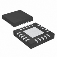
MAX7314ATG+ Maxim Integrated Products, MAX7314ATG+ Datasheet - Page 14

MAX7314ATG+
Manufacturer Part Number
MAX7314ATG+
Description
IC I/O EXPANDER I2C 16B 24TQFN
Manufacturer
Maxim Integrated Products
Datasheet
1.MAX7314AEG.pdf
(25 pages)
Specifications of MAX7314ATG+
Interface
I²C
Number Of I /o
18
Interrupt Output
Yes
Frequency - Clock
400kHz
Voltage - Supply
2 V ~ 3.6 V
Operating Temperature
-40°C ~ 125°C
Mounting Type
Surface Mount
Package / Case
24-TQFN Exposed Pad
Mounting Style
SMD/SMT
Lead Free Status / RoHS Status
Lead free / RoHS Compliant
In blink mode, the output ports can be flipped between
using either the blink phase 0 registers or the blink
phase 1 registers. Flip control is both hardware (the
BLINK input) and software control (the blink flip flag B
in the configuration register) (Table 4).
The blink function can be used for LED effects by pro-
gramming different display patterns in the two sets of
output port registers, and using the software or hard-
ware controls to flip between the patterns.
If the blink phase 1 registers are written with 0xFF, then
the BLINK input can be used as a hardware disable to,
for example, instantly turn off an LED pattern pro-
grammed into the blink phase 0 registers. This tech-
nique can be further extended by driving the BLINK
input with a PWM signal to modulate the LED current to
provide fading effects.
The blink mode is enabled by setting the blink enable flag
E in the configuration register (Table 4). When blink mode
is enabled, the states of the blink flip flag and the BLINK
input are EXOR’ed to set the phase, and the output ports
are set by either the blink phase 0 registers or the blink
phase 1 registers (Figure 11) (Table 7).
18-Port GPIO with LED Intensity Control,
Interrupt, and Hot-Insertion Protection
Table 4. Configuration Register (continued)
X = Don’t care.
14
outp ut i s l ow w hen i nter r up t enab l e ( I b i t) i s set
Read b ack d ata chang e i nter r up t status
—d ata chang e i s d etected , and INT/O16
Read b ack d ata chang e i nter r up t status
Read back BLINK input pin status—
Read back BLINK input pin status—
INT/O16 outp ut i s hi g h w hen i nter r up t
— d ata chang e i s not d etected , and
______________________________________________________________________________________
Read back device configuration
Write device configuration
CONFIGURATION
enab l e ( I b i t) i s set
input is high
REGISTER
input is low
R/W
0
1
1
1
1
1
Blink Mode
ADDRESS
CODE
(hex)
0x0F
INT
D7
X
X
0
1
The blink mode is disabled by clearing the blink enable
flag E in the configuration register (Table 4). When blink
mode is disabled, the state of the blink flip flag is
ignored, and the blink phase 0 registers alone control
the output ports.
When the blink function is disabled, the two blink phase
0 registers set the logic levels of the 16 ports (P0
through P15) when configured as outputs (Table 8). A
duplicate pair of registers called the blink phase 1 reg-
isters are also used if the blink function is enabled (Table
9). A logic high sets the appropriate output port high
impedance, while a logic low makes the port go low.
Figure 11. Blink Logic
BLINK ENABLE FLAG E
BLINK
BLINK FLIP FLAG B
D6
X
X
0
1
BLINK INPUT
O1
D5
X
X
X
X
REGISTER DATA
O0
D4
X
X
X
X
Blink Phase Registers
D3
X
X
X
X
I
D2
G
X
X
X
X
BLINK PHASE REGISTERS
D1
B
X
X
X
X
D0
E
X
X
X
X


