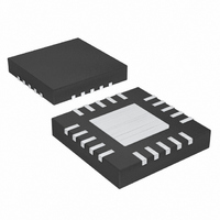
MAX7314ATG+ Maxim Integrated Products, MAX7314ATG+ Datasheet - Page 16

MAX7314ATG+
Manufacturer Part Number
MAX7314ATG+
Description
IC I/O EXPANDER I2C 16B 24TQFN
Manufacturer
Maxim Integrated Products
Datasheet
1.MAX7314AEG.pdf
(25 pages)
Specifications of MAX7314ATG+
Interface
I²C
Number Of I /o
18
Interrupt Output
Yes
Frequency - Clock
400kHz
Voltage - Supply
2 V ~ 3.6 V
Operating Temperature
-40°C ~ 125°C
Mounting Type
Surface Mount
Package / Case
24-TQFN Exposed Pad
Mounting Style
SMD/SMT
Lead Free Status / RoHS Status
Lead free / RoHS Compliant
Each output’s individual 4-bit intensity control only
operates during the number of timeslots gated by the
master intensity. The individual controls provide 16
intensity settings from 1/16 through 16/16 (Table 14).
Figures 16, 17, and 18 show examples of individual
intensity control settings. The highest value an individ-
ual or global setting can be set to is 16/16. This setting
forces the output to ignore the master control, and fol-
low the logic level set by the appropriate blink phase
register bit. The output becomes a glitch-free static out-
put with no PWM.
When blink is disabled (Table 7), the blink phase 0 reg-
isters specify each output’s logic level during the PWM
on-time (Table 8). The effect of setting an output’s blink
phase 0 register bit to zero or 1 is shown in Table 11.
With its output bit set to zero, an LED can be controlled
with 16 intensity settings from 1/16th duty through fully
on, but cannot be turned fully off using the PWM inten-
sity control. With its output bit set to 1, an LED can be
controlled with 16 intensity settings from fully off
through 15/16th duty.
18-Port GPIO with LED Intensity Control,
Interrupt, and Hot-Insertion Protection
Table 8. Blink Phase 0 Registers
Table 9. Blink Phase 1 Registers
16
Using PWM Intensity Controls with Blink Disabled
Read back outputs P15–P8 phase 0
Read back outputs P15–P8 phase 1
Read back outputs P7–P0 phase 0
Read back outputs P7–P0 phase 1
______________________________________________________________________________________
Write outputs P15–P8 phase 0
Write outputs P15–P8 phase 1
Write outputs P7–P0 phase 0
Write outputs P7–P0 phase 1
REGISTER
REGISTER
R/W
R/W
0
1
0
1
0
1
0
1
ADDRESS
ADDRESS
CODE
CODE
(hex)
(hex)
0x0A
0x0B
0x02
0x03
OP15
OP15
OP7
OP7
D7
D7
When blink is enabled (Table 7), the blink phase 0 regis-
ters and blink phase 1 registers specify each output’s
logic level during the PWM on-time during the respective
blink phases (Tables 8 and 9). The effect of setting an
output’s blink phase x register bit to zero or 1 is shown in
Table 12. LEDs can be flipped between either directly on
and off, or between a variety of high/low PWM intensities.
The 4 bits used for output O16’s PWM individual inten-
sity setting also double as the global intensity control
(Table 13). Global intensity simplifies the PWM settings
when the application requires them all to be the same,
such as for backlight applications, by replacing the 17
individual settings with 1 setting. Global intensity is
enabled with the global intensity flag G in the configura-
tion register (Table 4). When global PWM control is
used, the 4 bits of master intensity and 4 bits of global
intensity effectively combine to provide an 8-bit, 240-
step intensity control applying to all outputs.
It is not possible to apply global PWM control to a sub-
set of the ports, and use the others as logic outputs. To
mix static logic outputs and PWM outputs, individual
PWM control must be selected (Table 10).
Using PWM Intensity Controls with Blink Enabled
OP14
OP14
OP6
OP6
D6
D6
OP13
OP13
OP5
OP5
D5
D5
REGISTER DATA
REGISTER DATA
OP12
OP12
OP4
OP4
D4
D4
Global/O16 Intensity Control
OP11
OP11
OP3
OP3
D3
D3
OP10
OP10
OP2
OP2
D2
D2
OP1
OP9
OP1
OP9
D1
D1
OP0
OP8
OP0
OP8
D0
D0


