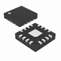
MAX7317ATE+T Maxim Integrated Products, MAX7317ATE+T Datasheet - Page 10

MAX7317ATE+T
Manufacturer Part Number
MAX7317ATE+T
Description
IC I/O EXPANDER SPI 10B 16TQFN
Manufacturer
Maxim Integrated Products
Datasheet
1.MAX7317AEE.pdf
(12 pages)
Specifications of MAX7317ATE+T
Interface
SPI/Microwire
Number Of I /o
10
Interrupt Output
No
Voltage - Supply
2.25 V ~ 3.6 V
Operating Temperature
-40°C ~ 125°C
Mounting Type
Surface Mount
Package / Case
16-TQFN Exposed Pad
Lead Free Status / RoHS Status
Lead free / RoHS Compliant
Frequency - Clock
-
The I/O ports P0–P9 remain high impedance with up to
8V asserted on them when the MAX7317 is powered
down (V+ = 0V). The MAX7317 can therefore be used
in hot-swap applications.
The MAX7317’s SPI interface is guaranteed to operate
at 26Mbps on a 2.5V supply, and on a 3.3V supply typi-
cally operates at 35Mbps. This means that transmission
line issues should be considered when the interface
connections are longer than 100mm, particularly with
higher supply voltages. Avoid running long adjacent
tracks for SCLK, DIN, and CS without interleaving GND
traces; otherwise, the signals may cross-couple, giving
false clock or chip-select transitions. Ringing may man-
ifest itself as communication issues, often intermittent,
typically due to double clocking caused by ringing at
the SCLK input. Fit a 1kΩ to 10kΩ parallel termination
resistor to either GND or V+ at the DIN, SCLK, and CS
inputs to damp ringing for moderately long interface
runs. Use line-impedance-matching terminations when
making connections between boards.
The open-drain output architecture allows the ports to
level translate the outputs to higher or lower voltages
than the MAX7317 supply. An external pullup resistor
can be used on any output to convert the high-imped-
ance logic-high condition to a positive voltage level.
The resistor can be connected to any voltage up to 7V.
When using a pullup on a constant-current output,
select the resistor value to sink no more than a few hun-
dred µA in logic-low condition. This ensures that the
current sink output saturates close to GND. For inter-
facing CMOS inputs, a pullup resistor value of 220kΩ is
a good starting point. Use a lower resistance to
10-Port SPI-Interfaced I/O Expander with
Overvoltage and Hot-Insertion Protection
Figure 6. Transmission of More than 16 Bits to the MAX7317
10
DOUT
SCLK
DIN
CS
______________________________________________________________________________________
BIT
1
Applications Information
BIT
2
SPI Routing Considerations
N-15
Output-Level Translation
N-31
N-14
N-30
N-13
N-29
Hot Insertion
N-28
N-12
N-27
N-11
N-26
N-10
N-25
N-9
improve noise immunity in applications where power
consumption is less critical, or where a faster rise time
is needed for a given capacitive load.
The MAX7317 operates with a power-supply voltage of
2.25V to 3.6V. Bypass the power supply to GND with a
0.047µF ceramic capacitor as close to the device as
possible. For the QFN version, connect the underside
exposed pad to GND.
TRANSISTOR COUNT: 14,865
PROCESS: BiCMOS
N-8
N-24
N-7
N-23
TOP VIEW
Pin Configurations (continued)
.
N-22
N-6
SCLK
GND
N-21
CS
N-5
P0
P1
P2
P3
P4
Power-Supply Considerations
1
2
6
3
4
5
7
8
N-20
N-4
MAX7317AEE
QSOP
N-19
N-3
Chip Information
N-18
N-2
16
15
14
13
12
11
10
9
N-17
N-1
V+
DIN
DOUT
P9
P8
P7
P6
P5
N-16
N


