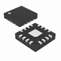
MAX7317ATE+T Maxim Integrated Products, MAX7317ATE+T Datasheet - Page 8

MAX7317ATE+T
Manufacturer Part Number
MAX7317ATE+T
Description
IC I/O EXPANDER SPI 10B 16TQFN
Manufacturer
Maxim Integrated Products
Datasheet
1.MAX7317AEE.pdf
(12 pages)
Specifications of MAX7317ATE+T
Interface
SPI/Microwire
Number Of I /o
10
Interrupt Output
No
Voltage - Supply
2.25 V ~ 3.6 V
Operating Temperature
-40°C ~ 125°C
Mounting Type
Surface Mount
Package / Case
16-TQFN Exposed Pad
Lead Free Status / RoHS Status
Lead free / RoHS Compliant
Frequency - Clock
-
Alternatively, MAX7317s can be daisy-chained by con-
necting the DOUT of one device to the DIN of the next,
and driving SCLK and CS lines in parallel (Figure 3).
This connection allows the MAX7317s to be read. Data
at DIN propagates through the internal shift registers
and appears at DOUT 15.5 clock cycles later, clocked
out on the falling edge of SCLK. When sending com-
mands to daisy-chained MAX7317s, all devices are
accessed at the same time. An access requires (16 x n)
clock cycles, where n is the number of MAX7317s con-
nected together. The serial interface speed (maximum
SCLK) is limited to 10MHz when multiple devices are
daisy-chained due to the DOUT propagation delay and
DIN setup time.
The MAX7317 is written to using the following
sequence (Figure 5):
1) Take SCLK low.
2) Take CS low. This enables the internal 16-bit shift
3) Clock 16 bits of data into DIN, D15 first to D0 last,
4) Take CS high (either while SCLK is still high after
5) Take SCLK low (if not already low).
10-Port SPI-Interfaced I/O Expander with
Overvoltage and Hot-Insertion Protection
Table 5. Serial-Data Format
Figure 2. MAX7317 Multiple CS Connection
8
R/ W
D15
register.
observing the setup and hold times. Bit D15 is low,
indicating a write command.
clocking in the last data bit, or after taking SCLK low).
_______________________________________________________________________________________
MSB
D14
D13
µC
D12
MOSI
SCLK
CS3
CS2
CS1
ADDRESS
D11
CS1
DIN
SCLK
D10
MAX7317
D9
LSB
D8
MSB
If fewer or greater than 16 bits are clocked into the
MAX7317 between taking CS low and taking CS high
again, the MAX7317 stores the last 16 bits received,
including the previous transmission(s). The general
case is when n bits (where n > 16) are transmitted to
the MAX7317. The last bits comprising bits {n-15} to
{n}, are retained, and are parallel loaded into the 16-bit
latch as bits D15 to D0, respectively (Figure 6).
Any register data within the MAX7317 can be read by
sending a logic high to bit D15. The sequence is:
1) Take SCLK low.
2) Take CS low. This enables the internal 16-bit shift
3) Clock 16 bits of data into DIN, D15 first to D0 last.
4) Take CS high (either while SCLK is still high after
5) Take SCLK low (if not already low).
6) Issue another read or write command, and examine
D7
register.
D15 is high, indicating a read command and bits
D14 through D8 contain the address of the register
to read. Bits D7 to D0 contain dummy data, which is
discarded.
clocking in the last data bit, or after taking SCLK
low). Positions D7 through D0 in the shift register are
now loaded with the register data addressed by bits
D15 through D8.
the bit stream at DOUT; the second 8 bits are the
contents of the register addressed by bits D14
through D8 in step 3.
CS2
DIN
SCLK
D6
MAX7317
D5
D4
Reading Device Registers
DATA
D3
CS3
DIN
SCLK
D2
MAX7317
D1
LSB
D0


