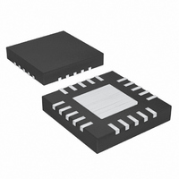
MAX7326ATG+T Maxim Integrated Products, MAX7326ATG+T Datasheet - Page 2

MAX7326ATG+T
Manufacturer Part Number
MAX7326ATG+T
Description
IC I/O EXPANDER I2C 16B 24TQFN
Manufacturer
Maxim Integrated Products
Datasheet
1.MAX7326ATG.pdf
(20 pages)
Specifications of MAX7326ATG+T
Interface
I²C
Number Of I /o
16
Interrupt Output
Yes
Frequency - Clock
400kHz
Voltage - Supply
1.71 V ~ 5.5 V
Operating Temperature
-40°C ~ 125°C
Mounting Type
Surface Mount
Package / Case
24-TQFN Exposed Pad
Includes
POR
Lead Free Status / RoHS Status
Lead free / RoHS Compliant
ABSOLUTE MAXIMUM RATINGS
(All voltages referenced to GND.)
Supply Voltage V+....................................................-0.3V to +6V
SCL, SDA, AD0, AD2, RST, INT, I2–I5......................-0.3V to +6V
O0, O1, O6–O15 .............................................-0.3V to V+ + 0.3V
O0, O1, O6–O15 Output Current......................................±25mA
SDA Sink Current ............................................................... 10mA
INT Sink Current..................................................................10mA
Total V+ Current..................................................................50mA
Total GND Current ...........................................................100mA
I
and 4 Inputs
ELECTRICAL CHARACTERISTICS
(V+ = +1.71V to +5.5V, T
Stresses beyond those listed under “Absolute Maximum Ratings” may cause permanent damage to the device. These are stress ratings only, and functional
operation of the device at these or any other conditions beyond those indicated in the operational sections of the specifications is not implied. Exposure to
absolute maximum rating conditions for extended periods may affect device reliability.
2
Operating Supply Voltage
Power-On Reset Voltage
Standby Current (Interface Idle)
Supply Current (Interface Running)
Input High Voltage
SDA, SCL, AD0, AD2, RST, I2–I5
Input Low Voltage
SDA, SCL, AD0, AD2, RST, I2–I5
Input Leakage Current
SDA, SCL, AD0, AD2, RST, I2–I5
Input Capacitance
SDA, SCL, AD0, AD2, RST, I2–I5
Output Low Voltage
O0, O1, O6–O15
Output High Voltage
O0, O1, O6–O15
Output Low Voltage SDA
Output Low Voltage INT
Port Input Pullup Resistor
2
_______________________________________________________________________________________
C Port Expander with 12 Push-Pull Outputs
PARAMETER
A
= -40°C to +125°C, unless otherwise noted. Typical values are at V+ = +3.3V, T
SYMBOL
V
V
I
V
OLSDA
IH
I
V
OLINT
V
R
V
V+
STB
V
POR
I+
OL
OH
, I
PU
IH
IL
IL
T
V+ falling
SCL and SDA and other digital inputs at V+
f
V+ < 1.8V
V+ ≥ 1.8V
V+ < 1.8V
V+ ≥ 1.8V
SDA, SCL, AD0, AD2, RST, I2–I5 at V+ or
GND
V+ = +1.71V, I
V+ = +2.5V, I
V+ = +3.3V, I
V+ = +5V, I
V+ = +1.71V, I
V+ = +2.5V, I
V+ = +3.3V, I
V+ = +5V, I
I
I
SCL
SINK
SINK
A
= -40°C to +125°C
= 400kHz, other digital inputs at V+
= 6mA
= 5mA
SINK
SOURCE
SINK
SINK
SOURCE
SOURCE
SINK
SOURCE
CONDITIONS
= 20mA
= 10mA
= 15mA
Continuous Power Dissipation (T
Operating Temperature Range .........................-40°C to +125°C
Junction Temperature ......................................................+150°C
Storage Temperature Range .............................-65°C to +150°C
Lead Temperature (soldering, 10s) .................................+300°C
= 5mA
= 10mA
24-Pin QSOP (derate 9.5mW/°C over +70°C) ............761.9mW
24-Pin TQFN (derate 20.8mW/°C over +70°C) ........1666.7mW
= 5mA
= 5mA
= 2mA
QSOP
TQFN
QSOP
TQFN
QSOP
TQFN
QSOP
TQFN
0.8 x V+
0.7 x V+
V+ - 250 V+ - 30
V+ - 360 V+ - 30
V+ - 260 V+ - 30
V+ - 360 V+ - 30
1.71
MIN
-0.2
25
A
= +70°C)
A
TYP
110
110
130
130
140
140
130
= +25°C.) (Note 1)
0.6
23
10
90
90
40
0.2 x V+
0.3 x V+
MAX
+0.2
5.50
180
230
210
260
230
280
250
300
250
250
1.6
1.9
55
55
UNITS
mV
mV
mV
mV
kΩ
µA
µA
µA
pF
V
V
V
V


