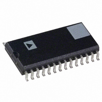
AD9814JRRL Analog Devices Inc, AD9814JRRL Datasheet - Page 3

AD9814JRRL
Manufacturer Part Number
AD9814JRRL
Description
IC CCD SIGNAL PROC 14BIT 28-SOIC
Manufacturer
Analog Devices Inc
Type
CCD Signal Processor, 14-Bitr
Specifications of AD9814JRRL
Rohs Status
RoHS non-compliant
Input Type
Logic
Output Type
Logic
Interface
3-Wire Serial
Current - Supply
80mA
Mounting Type
Surface Mount
Package / Case
28-SOIC (7.5mm Width)
Analog Front End Type
CCD
Analog Front End Category
Video
Interface Type
Serial (3-Wire)
Sample Rate
10MSPS
Operating Supply Voltage (min)
3/4.75V
Operating Supply Voltage (typ)
5V
Operating Supply Voltage (max)
5.25V
Resolution
14b
Supply Current
64/1.8mA
Number Of Adc's
1
Power Supply Type
Analog/Digital
Operating Temp Range
0C to 70C
Operating Temperature Classification
Commercial
Mounting
Surface Mount
Pin Count
28
Package Type
SOIC W
Number Of Channels
1
Lead Free Status / RoHS Status
Not Compliant
NOTES
1
2
3
4
5
Specifications subject to change without notice.
REV. 0
DIGITAL SPECIFICATIONS
Parameter
LOGIC INPUTS
LOGIC OUTPUTS
Specifications subject to change without notice.
TIMING SPECIFICATIONS
Parameter
CLOCK PARAMETERS
SERIAL INTERFACE
DATA OUTPUT
Specifications subject to change without notice.
The Integral Nonlinearity in measured using the “fixed endpoint” method, NOT using a “best-fit” calculation. See Definitions of Specifications.
The Gain Error specification is dominated by the tolerance of the internal differential voltage reference.
Linear input signal range is from 0 V to 4 V when the CCD’s reference level is clamped to 4 V by the AD9814’s input clamp. A larger reset transient can be tolerated
The input limits are defined as the maximum tolerable voltage levels into the AD9814. These levels are not intended to be in the linear input range of the device.
The PGA Gain is approximately “linear in dB” and follows the equation: Gain
by using the 3 V clamp level instead of the nominal 4 V clamp level. Linear input signal range will be from 0 V to 3 V when using the 3 V clamp level.
Signals beyond the input limits will turn on the overvoltage protection diodes.
3-Channel Pixel Rate
1-Channel Pixel Rate
ADCCLK Pulsewidth
CDSCLK1 Pulsewidth
CDSCLK2 Pulsewidth
CDSCLK1 Falling to CDSCLK2 Rising
ADCCLK Falling to CDSCLK2 Rising
CDSCLK2 Rising to ADCCLK Rising
CDSCLK2 Falling to ADCCLK Falling
CDSCLK2 Falling to CDSCLK1 Rising
ADCCLK Falling to CDSCLK1 Rising
Aperture Delay for CDS Clocks
Maximum SCLK Frequency
SLOAD to SCLK Set-Up Time
SCLK to SLOAD Hold Time
SDATA to SCLK Rising Set-Up Time
SCLK Rising to SDATA Hold Time
SCLK Falling to SDATA Valid
Output Delay
3-State to Data Valid
Output Enable High to 3-State
Latency (Pipeline Delay)
High Level Input Voltage
Low Level Input Voltage
High Level Input Current
Low Level Input Current
Input Capacitance
High Level Output Voltage
Low Level Output Voltage
High Level Output Current
Low Level Output Current
RESET TRANSIENT
1V TYP
(T
(T
C
MIN
L
MIN
= 10 pF, unless otherwise noted.)
to T
Symbol
V
V
I
I
C
V
V
I
I
to T
IH
IL
OH
OL
IH
IL
OH
OL
IN
MAX
MAX
, AVDD = +5 V, DRVDD = +5 V)
, AVDD = +5 V, DRVDD = +5 V, CDS Mode, f
4V p-p MAX INPUT SIGNAL RANGE
4V SET BY INPUT CLAMP (3V OPTION ALSO AVAILABLE)
GND
Symbol
t
t
t
t
t
t
t
t
t
t
t
t
f
t
t
t
t
t
t
t
t
PRA
PRB
ADCLK
C1
C2
C1C2
ADC2
C2ADR
C2ADF
C2C1
ADC1
AD
SCLK
LS
LH
DS
DH
RDV
OD
DV
HZ
Min
2.6
4.5
–3–
[
1
4 8
. [
5 8
.
Min
300
140
45
20
40
0
10
10
50
50
0
10
10
10
10
10
10
63 – G
63
]
]
where G is the register value. See Figure 13.
Typ
10
10
10
50
50
Typ
500
3
6
16
5
3 (Fixed)
ADCCLK
= 6 MHz, f
CDSCLK1
Max
0.8
0.1
Max
= f
CDSCLK2
AD9814
= 2 MHz,
Units
V
V
pF
V
V
Units
ns
ns
ns
ns
ns
ns
ns
ns
ns
ns
ns
ns
MHz
ns
ns
ns
ns
ns
ns
ns
ns
Cycles
A
A
A
A


