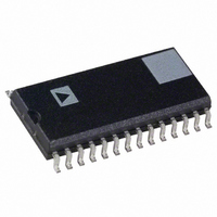
AD9814JRRL Analog Devices Inc, AD9814JRRL Datasheet - Page 9

AD9814JRRL
Manufacturer Part Number
AD9814JRRL
Description
IC CCD SIGNAL PROC 14BIT 28-SOIC
Manufacturer
Analog Devices Inc
Type
CCD Signal Processor, 14-Bitr
Specifications of AD9814JRRL
Rohs Status
RoHS non-compliant
Input Type
Logic
Output Type
Logic
Interface
3-Wire Serial
Current - Supply
80mA
Mounting Type
Surface Mount
Package / Case
28-SOIC (7.5mm Width)
Analog Front End Type
CCD
Analog Front End Category
Video
Interface Type
Serial (3-Wire)
Sample Rate
10MSPS
Operating Supply Voltage (min)
3/4.75V
Operating Supply Voltage (typ)
5V
Operating Supply Voltage (max)
5.25V
Resolution
14b
Supply Current
64/1.8mA
Number Of Adc's
1
Power Supply Type
Analog/Digital
Operating Temp Range
0C to 70C
Operating Temperature Classification
Commercial
Mounting
Surface Mount
Pin Count
28
Package Type
SOIC W
Number Of Channels
1
Lead Free Status / RoHS Status
Not Compliant
FUNCTIONAL DESCRIPTION
The AD9814 can be operated in four different modes: 3-Channel
CDS Mode, 3-Channel SHA Mode, 1-Channel CDS Mode,
and 1-Channel SHA Mode. Each mode is selected by program-
ming the Configuration Register through the serial interface.
For more detail on CDS or SHA mode operation, see the
Circuit Operation section.
3-Channel CDS Mode
In 3-Channel CDS Mode, the AD9814 simultaneously samples
the red, green and blue input voltages from the CCD outputs.
The sampling points for each Correlated Double Sampler (CDS)
are controlled by CDSCLK1 and CDSCLK2 (see Figures 8 and
9). CDSCLK1’s falling edge samples the reference level of the
CCD waveform. CDSCLK2’s falling edge samples the data
level of the CCD waveform. Each CDS amplifier outputs the
difference between the CCD’s reference and data levels. Next,
the output voltage of each CDS amplifier is level-shifted by an
Offset DAC. The voltages are then scaled by the three Program-
mable Gain Amplifiers before being multiplexed through the
14-bit ADC. The ADC sequentially samples the PGA outputs
on the falling edges of ADCCLK.
The offset and gain values for the red, green and blue channels
are programmed using the serial interface. The order in which
the channels are switched through the multiplexer is selected by
programming the MUX register.
Timing for this mode is shown in Figure 1. It is recommended
that the falling edge of CDSCLK2 occur coincident with or
before the rising edge of ADCCLK, although this is not re-
quired to satisfy the minimum timing constraints. The rising
edge of CDSCLK2 should not occur before the previous falling
edge of ADCCLK, as shown by t
is three clock cycles.
3-Channel SHA Mode
In 3-Channel SHA Mode, the AD9814 simultaneously samples
the red, green and blue input voltages. The sampling point is
controlled by CDSCLK2. CDSCLK2’s falling edge samples the
input waveforms on each channel. The output voltages from the
three SHAs are modified by the offset DACs and then scaled by
the three PGAs. The outputs of the PGAs are then multiplexed
through the 14-bit ADC. The ADC sequentially samples the
PGA outputs on the falling edges of ADCCLK.
The input signal is sampled with respect to the voltage applied
to the OFFSET pin (see Figure 10). With the OFFSET pin
REV. 0
ADC2
. The output data latency
–9–
grounded, a zero volt input corresponds to the ADC’s zero-scale
output. The OFFSET pin may also be used as a coarse offset
adjust pin. A voltage applied to this pin will be subtracted from
the voltages applied to the red, green and blue inputs in the first
amplifier stage of the AD9814. The input clamp is disabled in this
mode. For more information, see the Circuit Operation section.
Timing for this mode is shown in Figure 2. CDSCLK1 should
be grounded in this mode. Although not required, it is recom-
mended that the falling edge of CDSCLK2 occur coincident
with or before the rising edge of ADCCLK. The rising edge of
CDSCLK2 should not occur before the previous falling edge of
ADCCLK, as shown by t
ADCCLK cycles.
The offset and gain values for the red, green and blue channels
are programmed using the serial interface. The order in which
the channels are switched through the multiplexer is selected by
programming the MUX register.
1-Channel CDS Mode
This mode operates in the same way as the 3-Channel CDS
mode. The difference is that the multiplexer remains fixed in
this mode, so only the channel specified in the MUX register is
processed.
Timing for this mode is shown in Figure 3. Although not re-
quired, it is recommended that the falling edge of CDSCLK2
occur coincident with or before the rising edge of ADCCLK.
1-Channel SHA Mode
This mode operates in the same way as the 3-Channel SHA
mode, except that the multiplexer remains stationary. Only the
channel specified in the MUX register is processed.
The input signal is sampled with respect to the voltage applied
to the OFFSET pin. With the OFFSET pin grounded, a zero
volt input corresponds to the ADC’s zero scale output. The
OFFSET pin may also be used as a coarse offset adjust pin. A
voltage applied to this pin will be subtracted from the voltages
applied to the red, green and blue inputs in the first amplifier
stage of the AD9814. The input clamp is disabled in this mode.
For more information, see the Circuit Operation section.
Timing for this mode is shown in Figure 4. CDSCLK1 should
be grounded in this mode of operation. Although not required,
it is recommended that the falling edge of CDSCLK2 occur
coincident with or before the rising edge of ADCCLK.
ADC2
. The output data latency is three
AD9814


