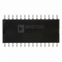
AD9822JRZ Analog Devices Inc, AD9822JRZ Datasheet - Page 13

AD9822JRZ
Manufacturer Part Number
AD9822JRZ
Description
IC CCD SIGNAL PROC 14BIT 28-SOIC
Manufacturer
Analog Devices Inc
Type
CCD Signal Processor, 14-Bitr
Datasheet
1.AD9822JRSZRL.pdf
(20 pages)
Specifications of AD9822JRZ
Input Type
Logic
Output Type
Logic
Interface
3-Wire Serial
Current - Supply
73mA
Mounting Type
Surface Mount
Package / Case
28-SOIC (7.5mm Width)
Analog Front End Type
CCD/CIS
Analog Front End Category
Video
Interface Type
Serial (3-Wire)
Sample Rate
15MSPS
Input Voltage Range
1V
Operating Supply Voltage (min)
3/4.75V
Operating Supply Voltage (typ)
5V
Operating Supply Voltage (max)
5.25V
Resolution
14b
Supply Current
4/73mA
Number Of Adc's
1
Power Supply Type
Analog/Digital
Operating Temp Range
0C to 70C
Operating Temperature Classification
Commercial
Mounting
Surface Mount
Pin Count
28
Package Type
SOIC W
Number Of Channels
3
Lead Free Status / RoHS Status
Lead free / RoHS Compliant
Available stocks
Company
Part Number
Manufacturer
Quantity
Price
Part Number:
AD9822JRZ
Manufacturer:
ADI/亚德诺
Quantity:
20 000
INTERNAL REGISTER DESCRIPTIONS
Table 6. Internal Register Map
Register Name
Configuration
MUX
Red PGA
Green PGA
Blue PGA
Red Offset
Green Offset
Blue Offset
Configuration Register
The Configuration Register controls the AD9822’s operating mode and bias levels. Bits D8, D1, and D0 should always be set low. Bit D7
sets the full-scale voltage range of the AD9822’s ADC to either 4 V (high) or 2 V (low). Bit D6 controls the internal voltage reference. If the
AD9822’s internal voltage reference is used, this bit is set high. Setting Bit D6 low disables the internal voltage reference, allowing an
external voltage reference to be used. Bit D5 configures the AD9822 for either the 3-channel (high) or 1-channel (low) mode of operation.
Setting Bit D4 high enables the CDS mode of operation and setting this bit low enables the SHA mode of operation. Bit D3 sets the dc bias
level of the AD9822’s input clamp. This bit should always be set high for the 4 V clamp bias, unless a CCD with a reset feedthrough
transient exceeding 2 V is used. If the 3 V clamp bias level is used, the peak-to-peak input signal range to the AD9822 is reduced to 3 V
maximum. Bit D2 controls the power-down mode. Setting Bit D2 high places the AD9822 into a very low power “sleep” mode. All register
contents are retained while the AD9822 is in the power-down state.
Table 7. Configuration Register Settings
D8
Set to 0
1
MUX Register
The MUX register controls the sampling channel order in the AD9822. Bits D8, D3, D2, D1, and D0 should always be set low. Bit D7 is
used when operating in 3-channel mode. Setting Bit D7 high sequences the MUX to sample the red channel first, then the green channel,
and then the blue channel. When in this mode, the CDSCLK2 pulse always resets the MUX to sample the red channel first (see Figure 3).
When Bit D7 is set low, the channel order is reversed to blue first, green second, and red third. The CDSCLK2 pulse always resets the
MUX to sample the blue channel first. Bits D6, D5, and D4 are used when operating in 1-channel mode. Bit D6 is set high to sample the
red channel. Bit D5 is set high to sample the green channel. Bit D4 is set high to sample the blue channel. The MUX remains stationary
during 1-channel mode.
Table 8. MUX Register Settings
D8
Set to 0
1
Power-on default value.
Power-on default value.
D7
Set to 0
D7
3-Channel Select
1 = R-G-B
0 = B-G-R
1
D6
Internal VREF
1 = Enabled
0 = Disabled
A2
0
0
0
0
1
1
1
1
Address
A1
0
0
1
1
0
0
1
1
D6
1-Channel Select
1 = RED
0 = Off
1
A0
0
1
0
1
0
1
0
1
D5
1 = 3-Ch Mode
0 = 1-Ch Mode
No. of Channels
1
D8
0
0
0
0
0
MSB
MSB
MSB
D7
0
RGB/BGR
0
0
0
D5
1-Channel Select
1 = GREEN
0 = Off
1
D4
1 = CDS Mode
0 = SHA Mode
CDS Operation
1
Rev. B | Page 13 of 20
D6
VREF
Red
0
0
0
1
D4
1-Channel Select
1 = BLUE
0 = Off
D
3Ch/1Ch
Green
MSB
MSB
MSB
D3
Input Clamp Bias
1 = 4 V
0 = 3 V
1
1
Data Bits
CDS On
D4
Blue
D3
Set to 0
D2
Power-Down
1 = On
0 = Off (Normal)
Clamp
D3
0
D2
Set to 0
D2
Pwr Dn
0
1
D1
Set to 0
D1
Set to 0
AD9822
D1
0
0
D0
Set to 0
D0
Set to 0
D0
0
0
LSB
LSB
LSB
LSB
LSB
LSB


