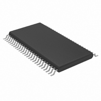
MAX9214EUM+TD Maxim Integrated Products, MAX9214EUM+TD Datasheet - Page 12

MAX9214EUM+TD
Manufacturer Part Number
MAX9214EUM+TD
Description
IC DESERIALIZER PROG 48TSSOP
Manufacturer
Maxim Integrated Products
Datasheet
1.MAX9220EUMTD.pdf
(17 pages)
Specifications of MAX9214EUM+TD
Function
Deserializer
Data Rate
1.785Gbps
Input Type
LVDS
Output Type
LVTTL, LVCMOS
Number Of Inputs
3
Number Of Outputs
21
Voltage - Supply
3 V ~ 3.6 V
Operating Temperature
-40°C ~ 85°C
Mounting Type
Surface Mount
Package / Case
48-TSSOP
Lead Free Status / RoHS Status
Lead free / RoHS Compliant
Programmable DC-Balance
21-Bit Deserializers
The transition time in a real system depends on the fre-
quency response of the cable driven by the serializer.
The capacitor value decreases for a higher frequency
parallel clock and for higher levels of droop and jitter.
Use high-frequency, surface-mount ceramic capacitors.
Equation 1 altered for four series capacitors (Figure 13) is:
The MAX9210/MAX9214/MAX9220/MAX9222 have fail-
safe LVDS inputs in non-DC-balanced mode (Figure 1).
Fail-safe drives the outputs low when the correspond-
ing LVDS input is open, undriven and shorted, or
undriven and parallel terminated. The fail-safe on the
LVDS clock input drives all outputs low. Fail-safe does
not operate in DC-balanced mode.
In DC-balanced mode, the inverting and noninverting
LVDS inputs are internally connected to +1.2V through
42kΩ (min) to provide biasing for AC-coupling (Figure 1).
A frequency-detection circuit on the clock input detects
when the input is not switching, or is switching at low
Figure 13. Four Capacitors per Link, AC-Coupled, DC-Balanced Mode
12
C = - (4 x t
______________________________________________________________________________________
Input Bias and Frequency Detection
PWRDWN
TxCLK IN
TxIN
B
x DSV)/(ln (1 - D) x (R
7
7
7
(7 + 2):1
(7 + 2):1
(7 + 2):1
PLL
21:3 SERIALIZER
MAX9209
MAX9213
T
+ R
O
)) (Eq 3)
Fail-Safe
TxOUT
TxCLK OUT
SURFACE-MOUNT CAPACITORS
HIGH-FREQUENCY CERAMIC
frequency. In this case, all outputs are driven low. To
prevent switching due to noise when the clock input is
not driven, bias the clock input to differential +15mV by
connecting a 10kΩ ±1% pullup resistor between the
noninverting input and V
resistor between the inverting input and ground. These
bias resistors, along with the 100Ω ±1% tolerance ter-
mination resistor, provide +15mV of differential input.
However, the +15mV bias causes degradation of
RSKM proportional to the slew rate of the clock input.
For example, if the clock transitions 250mV in 500ps,
the slew rate of 0.5mV/ps reduces RSKM by 30ps.
In non-DC-balanced mode, leave unused LVDS data
inputs open. In non-DC balanced mode, the input fail-
safe circuit drives the corresponding outputs low and no
pullup or pulldown resistors are needed. In DC-balanced
mode, at each unused LVDS data input, pull the inverting
input up to V
verting input down to ground using a 10kΩ resistor. Do
not connect a termination resistor. The pullup and pull-
down resistors drive the corresponding outputs low and
prevent switching due to noise.
100Ω
100Ω
100Ω
100Ω
RxCLK IN
RxIN
CC
using a 10kΩ resistor, and pull the nonin-
3:21 DESERIALIZER
MAX9210
MAX9214
MAX9220
MAX9222
Unused LVDS Data Inputs
CC
1:(9 - 2)
1:(9 - 2)
1:(9 - 2)
PLL
, and a 10kΩ ±1% pulldown
7
7
7
RxOUT
PWRDWN
RxCLK OUT


