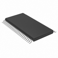
MAX9214EUM+TD Maxim Integrated Products, MAX9214EUM+TD Datasheet - Page 7

MAX9214EUM+TD
Manufacturer Part Number
MAX9214EUM+TD
Description
IC DESERIALIZER PROG 48TSSOP
Manufacturer
Maxim Integrated Products
Datasheet
1.MAX9220EUMTD.pdf
(17 pages)
Specifications of MAX9214EUM+TD
Function
Deserializer
Data Rate
1.785Gbps
Input Type
LVDS
Output Type
LVTTL, LVCMOS
Number Of Inputs
3
Number Of Outputs
21
Voltage - Supply
3 V ~ 3.6 V
Operating Temperature
-40°C ~ 85°C
Mounting Type
Surface Mount
Package / Case
48-TSSOP
Lead Free Status / RoHS Status
Lead free / RoHS Compliant
Table 1. DC-Balance Programming
The MAX9210/MAX9220 operate at a parallel clock fre-
quency of 8MHz to 34MHz in DC-balanced mode and
10MHz to 40MHz in non-DC-balanced mode. The
MAX9214/MAX9222 operate at a parallel clock frequency
of 16MHz to 66MHz in DC-balanced mode and 20MHz to
85MHz in non-DC-balanced mode. The transition times of
the single-ended outputs are increased on the
MAX9210/MAX9220 for reduced EMI.
DC-balanced or non-DC-balanced operation is con-
trolled by the DCB/NC pin (see Table 1 for DCB/NC
default settings and operating modes). In non-DC-bal-
anced mode, each channel deserializes 7 bits every
cycle of the parallel clock. In DC-balanced mode, 9 bits
are deserialized every clock cycle (7 data bits + 2 DC-
balance bits). The highest data rate in DC-balanced
mode for the MAX9214 and MAX9222 is 66MHz x 9 =
594Mbps. In non-DC-balanced mode, the maximum
data rate is 85MHz x 7 = 595Mbps.
Data coding by the MAX9209/MAX9213 serializers
(which are companion devices to the MAX9210/
MAX9214/MAX9220/MAX9222 deserializers) limits the
imbalance of ones and zeros transmitted on each chan-
nel. If +1 is assigned to each binary 1 transmitted and -1
is assigned to each binary 0 transmitted, the variation in
the running sum of assigned values is called the digital
sum variation (DSV). The maximum DSV for the data
channels is 10. At most, 10 more zeros than ones, or 10
more ones than zeros, are transmitted. The maximum
DSV for the clock channel is five. Limiting the DSV and
choosing the correct coupling capacitors maintains dif-
ferential signal amplitude and reduces jitter due to
droop on AC-coupled links.
MAX9210
MAX9214
MAX9220
MAX9222
DEVICE
_______________________________________________________________________________________
Detailed Description
High or open
High or open
High or open
High or open
DCB/NC
Low
Low
Low
Low
DC Balance
OUTPUT STROBE
Falling
Falling
EDGE
Rising
Rising
Programmable DC-Balance
Figure 1. LVDS Input Circuits
Figure 2. Worst-Case Test Pattern
RxIN_ + OR
EVEN RxOUT
RxIN_ - OR
RISING EDGE STROBE SHOWN.
RxCLK IN+
RxCLK IN-
ODD RxOUT
RxCLK OUT
RIN1
RIN1
NON-DC-BALANCED MODE
RIN2
OPERATING MODE
21-Bit Deserializers
Non-DC balanced
Non-DC balanced
Non-DC balanced
Non-DC balanced
V
CC
DC balanced
DC balanced
DC balanced
DC balanced
V
CC
- 0.3V
RCIP
RxIN_ + OR
RxIN_ - OR
RxCLK IN+
RxCLK IN-
RIN1
RIN1
DC-BALANCED MODE
FREQUENCY (MHz)
OPERATING
10 to 40
16 to 66
20 to 85
10 to 40
16 to 66
20 to 85
8 to 34
8 to 34
1.2V
7


