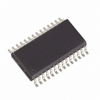
DS8113-RNG+ Maxim Integrated Products, DS8113-RNG+ Datasheet

DS8113-RNG+
Specifications of DS8113-RNG+
Related parts for DS8113-RNG+
DS8113-RNG+ Summary of contents
Page 1
... PIN Pads Automated Teller Machines Telecommunications Pay/Premium Television Ordering Information PART TEMP RANGE DS8113-RNG+ -40°C to +85°C DS8113-JNG+ -40°C to +85°C Note: Contact the factory for availability of other variants and package options. + Denotes a lead(Pb)-free/RoHS-compliant package. Selector Guide appears at end of data sheet. ...
Page 2
... I = 30mA 20MHz, CC XTAL I DD_IC f = 10MHz 5.0V (Note 2) CLK DDA Card inactive, active-high PRES DS8113 not in stop mode DS8113 in ultra-low-power stop I mode (CMDVCC, 5V/3V, and 1_8V DD_STOP set to logic 1) (Note 3) = -25°C to +85°C) .......700mW A MIN TYP MAX UNITS 2.7 6.0 V 5.0 6 ...
Page 3
RECOMMENDED DC OPERATING CONDITIONS (continued +3.3V +5.0V +25°C, unless otherwise noted.) (Note 1) DD DDA A PARAMETER CLOCK SOURCE Crystal Frequency XTAL1 Operating Conditions External Capacitance for Crystal Internal Oscillator SHUTDOWN TEMPERATURE Shutdown Temperature ...
Page 4
Smart Card Interface RECOMMENDED DC OPERATING CONDITIONS (continued +3.3V +5.0V +25°C, unless otherwise noted.) (Note 1) DD DDA A PARAMETER Output Low Voltage Card-Active Mode Output Current Shutdown Current Threshold Slew Rate DATA LINES ...
Page 5
RECOMMENDED DC OPERATING CONDITIONS (continued +3.3V +5.0V +25°C, unless otherwise noted.) (Note 1) DD DDA A PARAMETER I/OIN, AUX1IN, AUX2IN PINS Output Low Voltage Output High Voltage Output Rise/Fall Time Input Low Voltage Input ...
Page 6
... PRES/PRES Debounce Time Note 1: Operation guaranteed at -40°C and +85°C but not tested. Note 2: IDD_IC measures the amount of current used by the DS8113 to provide the smart card current minus the load. Note 3: Stop mode is enabled by setting CMDVCC, 5V/3V, and 1_8V to a logic-high. ...
Page 7
... XTAL1. 26 I/OIN I/O Input. Host-to-interface chip data I/O line. AUX1IN, 27, 28 C4/C8 Input. Host-to-interface I/O line for auxiliary connections to C4 and C8. AUX2IN _______________________________________________________________________________________ Smart Card Interface Pin Description FUNCTION . For the DS8113 this must be at least 5.0V. DD integrated pullup resistor to VDD. 7 ...
Page 8
... PDAs, consuming only 10nA in stop mode. See Figure 1 for a functional diagram. The DS8113 is a dual-supply device. The supply pins for the device are VDD, GND, VDDA, and PGND. V should be in the range of 2.7V to 6.0V, and is the sup- ply for signals that interface with the host controller ...
Page 9
... Current to and from the card I/O lines is limited internally to 15mA. The maximum frequency on these lines is 1MHz. The DS8113 powers up with the card interface in the inactive mode. Minimal circuitry is active while waiting for the host to initiate a smart card session. • All card contacts are inactive (approximately 200Ω ...
Page 10
... RSTIN can be set high to obtain an answer to request (ATR) from an inserted smart card. Do not perform acti- vation with RSTIN held permanently high 4T When the activation sequence is completed, the DS8113 card interface is in active mode. The host microcontroller and the smart card exchange data on the I/O lines ...
Page 11
CMDVCC VCC I/O CLK RSTIN RST I/OIN Figure 4. Activation Sequence CMDVCC RST CLK I/O VCC t 10 Figure 5. Deactivation Sequence ______________________________________________________________________________________ Smart Card Interface 200ns ...
Page 12
... PRES sig- nals at card insertion or withdrawal. The DS8113 has a debounce feature with an 8ms typi- cal duration (Figure 6). When a card is inserted, output OFF goes high after the debounce time delay. When ...
Page 13
PRES OFF CMDVCC DEBOUNCE VCC Figure 6. Behavior of PRES, OFF, CMDVCC, and VCC OFF PRES RST CLK I/O VCC t 10 Figure 7. Emergency Deactivation Sequence (Card Extraction) ______________________________________________________________________________________ Smart Card Interface DEBOUNCE DEACTIVATION CAUSED BY CARDS WITHDRAWAL t ...
Page 14
... This prevents smart card access from occurring after leaving the stop mode. Figure 8 shows the control sequence for entering and exiting stop mode. Note that an in-progress deactivation sequence always finishes before the DS8113 enters low-power stop mode. ACTIVATE DEACTIVATE STOP MODE STOP MODE 220μ ...
Page 15
... If both 1_8V CC voltages: CC and 5V/3V are high with CMDVCC high at the same time, the DS8113 enters stop mode. To avoid acciden- tal entry into stop mode, the state of 1_8V and 5V/3V must not be changed simultaneously. A minimum delay of 100ns should be observed between changing the CC states of 1_8V and 5V/3V ...
Page 16
... Selector Guide LOW STOP- LOW ACTIVE- PART MODE POWER MODE POWER DS8113-RNG+ Yes DS8113-JNG+ Yes Note: Contact the factory for availability of other variants and package options. + Denotes a lead(Pb)-free/RoHS-compliant package. Package Information For the latest package outline information and land patterns www.maxim-ic.com/packages. Note that a “ ...
Page 17
... Maxim cannot assume responsibility for use of any circuitry other than circuitry entirely embodied in a Maxim product. No circuit patent licenses are implied. Maxim reserves the right to change the circuitry and specifications without notice at any time. Maxim Integrated Products, 120 San Gabriel Drive, Sunnyvale, CA 94086 408-737-7600 ____________________ 17 © 2010 Maxim Integrated Products ...


