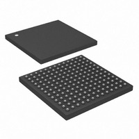
DS33Z11+ Maxim Integrated Products, DS33Z11+ Datasheet - Page 148

DS33Z11+
Manufacturer Part Number
DS33Z11+
Description
IC MAPPER ETHERNET 169-CSBGA
Manufacturer
Maxim Integrated Products
Datasheet
1.DS33Z11.pdf
(172 pages)
Specifications of DS33Z11+
Applications
Data Transport
Interface
SPI/Parallel
Voltage - Supply
1.8V, 3.3V
Package / Case
169-CSBGA
Mounting Type
Surface Mount
Lead Free Status / RoHS Status
Lead free / RoHS Compliant
- Current page: 148 of 172
- Download datasheet (2Mb)
Note 1: Typical power is 145mW.
Note 2: All outputs loaded with rated capacitance; all inputs between V
Note 3: RST pin held low, or RST bit set.
Note 4: RST pin held low, or RST bit set. All clocks stopped.
11.1 Thermal Characteristics
Note 1: The package is mounted on a four-layer JEDEC standard test board.
Note 2: Theta-JA (θ
standard test board.
11.2 Theta-JA vs. Airflow
Ambient Temperature (Note 1)
Junction Temperature
Theta-JA (θ
14mm CSBGA (Note 2)
Theta-JA (θ
10mm CSBGA (Note 2)
Input Leakage
Output Leakage (when Hi-Z)
Output Voltage (I
Output Voltage (I
Output Voltage (I
Output Voltage (I
Input Voltage
AIR FLOW
(m/s)
2.5
0
1
PARAMETER
PARAMETER
JA
JA
) in Still Air for 169-pin
) in Still Air for 100-pin
JA
OH
OL
OH
OL
169-Pin 14mm CSBGA
) is the junction-to-ambient thermal resistance, when the package is mounted on a four-layer JEDEC
= +4.0mA)
= +12.0mA)
= -4.0mA)
= -8.0mA)
(°C/W)
52.7
45.8
43.8
THETA-JA
SYMBOL
V
V
V
V
-40°C
V
I
V
I
MIN
ILP
LO
OH
OH
OL
OL
IH
IL
100-Pin 10mm CSBGA
148 of 172
All Outputs
All Outputs
REF_CLKO
TSER
CONDITIONS
(°C/W)
+52.7°C/W
+47.1°C/W
47.1
40.8
38.4
TYP
DD
and V
SS
; inputs with pullups connected to V
+125°C
+85°C
MIN
MAX
-50
-10
2.4
2.4
2.0
TYP
MAX
+10
-10
0.4
0.4
0.8
DD
UNITS
.
µA
µA
V
V
V
V
V
V
Related parts for DS33Z11+
Image
Part Number
Description
Manufacturer
Datasheet
Request
R

Part Number:
Description:
MAX7528KCWPMaxim Integrated Products [CMOS Dual 8-Bit Buffered Multiplying DACs]
Manufacturer:
Maxim Integrated Products
Datasheet:

Part Number:
Description:
Single +5V, fully integrated, 1.25Gbps laser diode driver.
Manufacturer:
Maxim Integrated Products
Datasheet:

Part Number:
Description:
Single +5V, fully integrated, 155Mbps laser diode driver.
Manufacturer:
Maxim Integrated Products
Datasheet:

Part Number:
Description:
VRD11/VRD10, K8 Rev F 2/3/4-Phase PWM Controllers with Integrated Dual MOSFET Drivers
Manufacturer:
Maxim Integrated Products
Datasheet:

Part Number:
Description:
Highly Integrated Level 2 SMBus Battery Chargers
Manufacturer:
Maxim Integrated Products
Datasheet:

Part Number:
Description:
Current Monitor and Accumulator with Integrated Sense Resistor; ; Temperature Range: -40°C to +85°C
Manufacturer:
Maxim Integrated Products

Part Number:
Description:
TSSOP 14/A�/RS-485 Transceivers with Integrated 100O/120O Termination Resis
Manufacturer:
Maxim Integrated Products

Part Number:
Description:
TSSOP 14/A�/RS-485 Transceivers with Integrated 100O/120O Termination Resis
Manufacturer:
Maxim Integrated Products

Part Number:
Description:
QFN 16/A�/AC-DC and DC-DC Peak-Current-Mode Converters with Integrated Step
Manufacturer:
Maxim Integrated Products

Part Number:
Description:
TDFN/A/65V, 1A, 600KHZ, SYNCHRONOUS STEP-DOWN REGULATOR WITH INTEGRATED SWI
Manufacturer:
Maxim Integrated Products

Part Number:
Description:
Integrated Temperature Controller f
Manufacturer:
Maxim Integrated Products

Part Number:
Description:
SOT23-6/I�/45MHz to 650MHz, Integrated IF VCOs with Differential Output
Manufacturer:
Maxim Integrated Products

Part Number:
Description:
SOT23-6/I�/45MHz to 650MHz, Integrated IF VCOs with Differential Output
Manufacturer:
Maxim Integrated Products

Part Number:
Description:
EVALUATION KIT/2.4GHZ TO 2.5GHZ 802.11G/B RF TRANSCEIVER WITH INTEGRATED PA
Manufacturer:
Maxim Integrated Products

Part Number:
Description:
QFN/E/DUAL PCIE/SATA HIGH SPEED SWITCH WITH INTEGRATED BIAS RESISTOR
Manufacturer:
Maxim Integrated Products
Datasheet:


