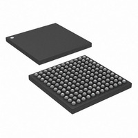
DS33X11+ Maxim Integrated Products, DS33X11+ Datasheet - Page 35

DS33X11+
Manufacturer Part Number
DS33X11+
Description
IC MAPPING ETHERNET 144CSBGA
Manufacturer
Maxim Integrated Products
Datasheet
1.DS33X11.pdf
(375 pages)
Specifications of DS33X11+
Applications
Data Transport
Interface
SPI
Voltage - Supply
1.8V, 2.5V, 3.3V
Package / Case
144-CSBGA
Mounting Type
Surface Mount
Lead Free Status / RoHS Status
Lead free / RoHS Compliant
- Current page: 35 of 375
- Download datasheet (3Mb)
8.1
Configuration and control can be accomplished through the 8-bit parallel microprocessor port. The device’s 16-bit
registers are accessed as sequential byte addresses. The 8-bit parallel data bus can be configured for Intel or
Motorola modes of operation. The 8-bit parallel data bus can be configured for Intel or Motorola modes of operation
with the MODE pin. When MODE = 0, bus timing is in Intel mode, as shown in Figure 12-13 and Figure 12-14.
When MODE = 1, bus timing is in Motorola mode, as shown in Figure 12-15 and Figure 12-16. The address space
is mapped through the use of 11 address lines, A0-A10. An address latch enable [ALE] pin is provided to allow for
multiplexing of the data and address signals. Note that the parallel bus is not available in the 144 pin DS33X11,
and the SPI Slave port must be used for processor control.
The Chip Select (CS) pin must be brought to a logic low level to gain read and write access to the microprocessor
port. With Intel timing selected, the Read (RD) and Write (WR) pins are used to indicate read and write operations
and latch data through the interface. With Motorola timing selected, the Read-Write (
read and write operations while the Data Strobe (DS) pin is used to latch data through the interface.
The interrupt output pin (INT) is an open-drain output that will assert a logic-low level upon a number of software
maskable interrupt conditions. The inactive state of this pin can be configured with the GL.CR2.INTM bit. This pin is
normally connected to the microprocessor interrupt input. The register map is shown in Table 10-1 on Page 105.
8.1.1
The processor interface can operate in either read-write strobe mode or data strobe mode. When MODE = 0 the
read-write strobe mode is enabled and a negative pulse on RD performs a read cycle, and a negative pulse on WR
performs a write cycle. When MODE pin = 1, the data strobe mode is enabled and a negative pulse on DS when
R
write strobe mode is commonly called the “Intel” mode, and the data strobe mode is commonly called the
“Motorola” mode.
8.1.2
The latched status registers will clear on a read access. It is important to note that in a multi-task software
environment, the user should handle all status conditions of each register at the same time to avoid inadvertently
clearing status conditions. The latched status register bits are carefully designed so that an event occurrence
cannot collide with a user read access.
8.1.3
The interrupt (INT) pin is configurable to drive high or float when not active. The GL.CR2.INTM bit controls the pin
configuration, when it is set to 1, the INT pin will drive high when inactive. After reset, the INT pin is in high
impedance mode until an interrupt source is active and enabled to drive the interrupt pin.
8.1.4
An address latch enable [ALE] pin is provided to allow for multiplexing of the data and address signals. For
multiplexed operation, each of the eight data lines (D0-D7) must be externally connected to each of the lower eight
address lines (A0-A7). The remaining address lines (A8-A10) are connected as normal. Address inputs are latched
upon the falling edge of the ALE signal. ALE must remain low until the read or write operation is complete.
Rev: 063008
W is high performs a read cycle, and a negative pulse on DS when
________________________________________________ DS33X162/X161/X82/X81/X42/X41/X11/W41/W11
Parallel Processor Interface
Read-Write/Data Strobe Modes
Clear on Read
Interrupt and Pin Modes
Multiplexed Bus Operation
R
W is low performs a write cycle. The read-
R
W) pin is used to indicate
35 of 375
Related parts for DS33X11+
Image
Part Number
Description
Manufacturer
Datasheet
Request
R

Part Number:
Description:
MAX7528KCWPMaxim Integrated Products [CMOS Dual 8-Bit Buffered Multiplying DACs]
Manufacturer:
Maxim Integrated Products
Datasheet:

Part Number:
Description:
Single +5V, fully integrated, 1.25Gbps laser diode driver.
Manufacturer:
Maxim Integrated Products
Datasheet:

Part Number:
Description:
Single +5V, fully integrated, 155Mbps laser diode driver.
Manufacturer:
Maxim Integrated Products
Datasheet:

Part Number:
Description:
VRD11/VRD10, K8 Rev F 2/3/4-Phase PWM Controllers with Integrated Dual MOSFET Drivers
Manufacturer:
Maxim Integrated Products
Datasheet:

Part Number:
Description:
Highly Integrated Level 2 SMBus Battery Chargers
Manufacturer:
Maxim Integrated Products
Datasheet:

Part Number:
Description:
Current Monitor and Accumulator with Integrated Sense Resistor; ; Temperature Range: -40°C to +85°C
Manufacturer:
Maxim Integrated Products

Part Number:
Description:
TSSOP 14/A�/RS-485 Transceivers with Integrated 100O/120O Termination Resis
Manufacturer:
Maxim Integrated Products

Part Number:
Description:
TSSOP 14/A�/RS-485 Transceivers with Integrated 100O/120O Termination Resis
Manufacturer:
Maxim Integrated Products

Part Number:
Description:
QFN 16/A�/AC-DC and DC-DC Peak-Current-Mode Converters with Integrated Step
Manufacturer:
Maxim Integrated Products

Part Number:
Description:
TDFN/A/65V, 1A, 600KHZ, SYNCHRONOUS STEP-DOWN REGULATOR WITH INTEGRATED SWI
Manufacturer:
Maxim Integrated Products

Part Number:
Description:
Integrated Temperature Controller f
Manufacturer:
Maxim Integrated Products

Part Number:
Description:
SOT23-6/I�/45MHz to 650MHz, Integrated IF VCOs with Differential Output
Manufacturer:
Maxim Integrated Products

Part Number:
Description:
SOT23-6/I�/45MHz to 650MHz, Integrated IF VCOs with Differential Output
Manufacturer:
Maxim Integrated Products

Part Number:
Description:
EVALUATION KIT/2.4GHZ TO 2.5GHZ 802.11G/B RF TRANSCEIVER WITH INTEGRATED PA
Manufacturer:
Maxim Integrated Products

Part Number:
Description:
QFN/E/DUAL PCIE/SATA HIGH SPEED SWITCH WITH INTEGRATED BIAS RESISTOR
Manufacturer:
Maxim Integrated Products
Datasheet:


