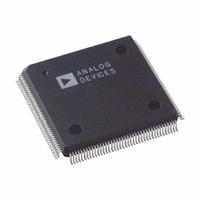
AD9887AKSZ-170 Analog Devices Inc, AD9887AKSZ-170 Datasheet - Page 35

AD9887AKSZ-170
Manufacturer Part Number
AD9887AKSZ-170
Description
IC INTRFACE ANALOG/DVI 160-MQFP
Manufacturer
Analog Devices Inc
Specifications of AD9887AKSZ-170
Applications
Graphic Cards, VGA Interfaces
Interface
Analog and Digital
Voltage - Supply
3.15 V ~ 3.45 V
Package / Case
160-MQFP, 160-PQFP
Mounting Type
Surface Mount
Supply Voltage Range
3.15V To 3.45V, 2.2V To 3.45V
Operating Temperature Range
0°C To +70°C
Digital Ic Case Style
MQFP
No. Of Pins
160
Msl
MSL 3 - 168 Hours
Termination Type
SMD
Rohs Compliant
Yes
Filter Terminals
SMD
Bandwidth
170MHz
Lead Free Status / RoHS Status
Lead free / RoHS Compliant
Available stocks
Company
Part Number
Manufacturer
Quantity
Price
Company:
Part Number:
AD9887AKSZ-170
Manufacturer:
ADI
Quantity:
437
Company:
Part Number:
AD9887AKSZ-170
Manufacturer:
Analog Devices Inc
Quantity:
10 000
Part Number:
AD9887AKSZ-170
Manufacturer:
AD
Quantity:
20 000
Address
0x22
0x23
0x24
0x25
0x26
0x27
1
2-WIRE SERIAL CONTROL REGISTER DETAILS
Chip Identification
0x00 7:0
PLL Divider Control
0x01 7:0
The AD9887A only updates the PLL divide ratio when the LSBs are written to Register 0x02.
Bit 7 through Bit 4 represent functional revisions to the
analog interface. Changes in these bits generally indicate
that software and/or hardware changes are required for
the chip to work properly. Bit 3 through Bit 0 represent
nonfunctional related revisions and are reset to 0000
when the MSBs are changed. Changes in these bits are
considered transparent to the user.
The 8 MSBs of the 12-bit PLL divide ratio PLLDIV. (The
operational divide ratio is PLLDIV + 1.)
The PLL derives a pixel clock from the incoming Hsync
signal. The pixel clock frequency is then divided by an
integer value, such that the output is phase-locked to
Hsync. This PLLDIV value determines the number of
pixel times (pixels plus horizontal blanking overhead)
per line. This is typically 20% to 30% more than the
number of active pixels in the display.
The 12-bit value of the PLL divider supports divide ratios
from 221 to 4095. The higher the value loaded in this
register, the higher the resulting clock frequency with
respect to a fixed Hsync frequency. VESA has established
standard timing specifications that help determine the value
for PLLDIV as a function of horizontal and vertical display
resolution and frame rate (Table 7). However, many com-
puter systems do not conform precisely to the recom-
mendations, and these numbers should be used only as a
guide. The display system manufacturer should provide
automatic or manual means for optimizing PLLDIV. An
incorrectly set PLLDIV usually produces one or more
vertical noise bars on the display. The greater the error, the
greater the number of bars produced. The power-up default
of PLLDIV is 1693 (PLLDIVM = 0x69, PLLDIVL = 0xDx).
The AD9887A updates the full divide ratio only when
the LSBs are changed. Writing to this register by itself
does not trigger an update.
Read and
Write, or
Read Only
R/W
R/W
R/W
R/W
R/W
Chip Revision
PLL Divide Ratio MSBs
Bits
7:0
7:0
7:0
7:0
7:0
Default
Value
00000000
00000000
00000000
11110000
11111111
00001111
Register Name
Rev. B | Page 35 of 52
Description
Must be set to default.
Must be set to 0x2A for proper operation.
Must be set to default.
Must be set to default.
Must be set to default.
Must be set to default
0x02 7:4
Clock Generator Controls
0x03 7
0x03 6:5
Table 10. VCO Ranges
VCORNGE
00
01
10
11
The 4 LSBs of the 12-bit PLL divide ratio PLLDIV. The
operational divide ratio is PLLDIV + 1.
The power-up default value of PLLDIV is 1693
(PLLDIVM = 0x69, PLLDIVL = 0xDx).
The AD9887A updates the full divide ratio only when
the user writes to this register.
Two bits that establish the operating range of the clock
generator.
VCORNGE must be set to correspond with the desired
operating frequency (incoming pixel rate).
Must be set to 1 for proper device operation.
The PLL provides the best jitter performance at high
frequencies. To output low pixel rates while minimizing
jitter, the PLL operates at a higher frequency and divides
down the clock rate afterwards. Table 10 shows the pixel
rates for each VCO range setting. The PLL output divisor
is automatically selected with the VCO range setting.
The power-up default value is 01.
Test
PLL Divide Ratio LSBs
VCO Range Select
Pixel Rate Range
12 to 37
37 to 74
74 to 140
140 to 170
AD9887A


