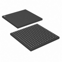
DS33X81+ Maxim Integrated Products, DS33X81+ Datasheet - Page 24

DS33X81+
Manufacturer Part Number
DS33X81+
Description
IC MAPPING ETHERNET 256CSBGA
Manufacturer
Maxim Integrated Products
Datasheet
1.DS33X11.pdf
(375 pages)
Specifications of DS33X81+
Applications
Data Transport
Interface
Parallel/Serial
Voltage - Supply
1.8V, 2.5V, 3.3V
Package / Case
256-CSBGA
Mounting Type
Surface Mount
Lead Free Status / RoHS Status
Lead free / RoHS Compliant
- Current page: 24 of 375
- Download datasheet (3Mb)
Rev: 063008
________________________________________________ DS33X162/X161/X82/X81/X42/X41/X11/W41/W11
RX_CRS1,
RX_ERR1,
TX_ERR1,
DCEDTES
RX_CRS2
RX_ERR2
TX_ERR2
RMII_SEL
RX_DV1,
TX_EN1,
RX_DV2
TX_EN2
NAME
COL1,
COL2
PACKAGE PINS
G15,
H15,
K14,
E13,
E14,
M11
M12
L14,
M14
P16
R16
P13
256
J14
L16
G12
G10
144
G9
G8
F8
F9
K7
L7
TYPE
O
O
I
I
I
I
I
I
Transmit Enable 1(GMII). When this signal is asserted, the data on
TXD[7:0] is valid.
Transmit Enable 1, 2 (MII/RMII). In MII mode, this pin is asserted high
when data TXD[3:0] is being provided by the device. In RMII mode, this
pin is asserted high when data TXD[1:0] is being provided by the device.
The signal is deasserted prior to the first nibble of the next frame. This
signal is synchronous with the rising edge TX_CLK. It is asserted with the
first bit of the preamble.
Note that TX_EN2 is only available on devices with two Ethernet ports.
Unused output pins should not be connected.
Receive Data Valid 1 (GMII). This signal is synchronous to the RX_CLK1
and provides a valid signal for the RXD[7:0].
Receive Data Valid 1, 2 (MII/RMII). This active-high signal indicates valid
data from the PHY. In MII mode the data RXD[3:0] is ignored if RX_DV is
not asserted high. In RMII mode the data RXD[1:0] is ignored if RX_DV is
not asserted high.
Note that RX_DV2 is only available on devices with two Ethernet ports.
Receive Carrier Sense 1 (GMII). This signal is asserted (high) when data
is valid from the PHY. This signal is asserted by the PHY when either
transmit or receive medium is active. This signal is not synchronous to
any of the clocks.
Receive Carrier Sense 1, 2 (MII). This signal is asserted by the PHY when
either transmit or receive medium is active. This signal is not synchronous
to any of the clocks.
Note that RX_CRS2 is only available on devices with two Ethernet ports.
Receive Error 1 (GMII). This signal indicates a receive error or a carrier
extension in the GMII Mode.
Receive Error 1, 2 (MII). Asserted by the MAC PHY for one or more
RX_CLK periods indicating that an error has occurred. Active High
indicates Receive code group is invalid. If RX_CRS is low, RX_ERR has
no effect. This is synchronous with RX_CLK. In DCE mode, this signal
must be grounded.
Note that RX_ERR2 is only available on devices with two Ethernet ports.
Transmit Error 1(GMII). When this signal is asserted, the PHY will
respond by sending one or more code groups in error.
Transmit Error 1, 2(GMII, MII). When this signal is asserted, the PHY will
respond by sending one or more code groups in error.
Note that TX_ERR2 is only available on devices with two Ethernet ports.
Collision Detect 1, 2 (MII). Asserted by the Ethernet PHY to indicate that
a collision is occurring. In DCE Mode this signal should be connected to
ground. This signal is only valid in half duplex mode, and is ignored in full
duplex mode.
Note that COL2 is only available on devices with two Ethernet ports.
DCE or DTE Selection (MII). Setting this pin high places all Ethernet
ports in DCE Mode. Setting this pin low places the Ethernet ports in DTE
Mode.
In DCE Mode, the MII interface can be directly connected to another
MAC. In DCE Mode, the Transmit clock (TX_CLK) and Receive clock
(RX_CLK) are outputs.
Note that there is no software bit selection of DCEDTES. Note that DCE
operation is only valid for 10/100, MII mode.
RMII Selection Input. Set this pin to 1 for RMII operation. In devices with
2 Ethernet ports, both ports will operate in RMII mode. REF_CLK must be
50MHz. Set this pin to 0 for GMII or MII operation.
FUNCTION
24 of 375
Related parts for DS33X81+
Image
Part Number
Description
Manufacturer
Datasheet
Request
R

Part Number:
Description:
MAX7528KCWPMaxim Integrated Products [CMOS Dual 8-Bit Buffered Multiplying DACs]
Manufacturer:
Maxim Integrated Products
Datasheet:

Part Number:
Description:
Single +5V, fully integrated, 1.25Gbps laser diode driver.
Manufacturer:
Maxim Integrated Products
Datasheet:

Part Number:
Description:
Single +5V, fully integrated, 155Mbps laser diode driver.
Manufacturer:
Maxim Integrated Products
Datasheet:

Part Number:
Description:
VRD11/VRD10, K8 Rev F 2/3/4-Phase PWM Controllers with Integrated Dual MOSFET Drivers
Manufacturer:
Maxim Integrated Products
Datasheet:

Part Number:
Description:
Highly Integrated Level 2 SMBus Battery Chargers
Manufacturer:
Maxim Integrated Products
Datasheet:

Part Number:
Description:
Current Monitor and Accumulator with Integrated Sense Resistor; ; Temperature Range: -40°C to +85°C
Manufacturer:
Maxim Integrated Products

Part Number:
Description:
TSSOP 14/A�/RS-485 Transceivers with Integrated 100O/120O Termination Resis
Manufacturer:
Maxim Integrated Products

Part Number:
Description:
TSSOP 14/A�/RS-485 Transceivers with Integrated 100O/120O Termination Resis
Manufacturer:
Maxim Integrated Products

Part Number:
Description:
QFN 16/A�/AC-DC and DC-DC Peak-Current-Mode Converters with Integrated Step
Manufacturer:
Maxim Integrated Products

Part Number:
Description:
TDFN/A/65V, 1A, 600KHZ, SYNCHRONOUS STEP-DOWN REGULATOR WITH INTEGRATED SWI
Manufacturer:
Maxim Integrated Products

Part Number:
Description:
Integrated Temperature Controller f
Manufacturer:
Maxim Integrated Products

Part Number:
Description:
SOT23-6/I�/45MHz to 650MHz, Integrated IF VCOs with Differential Output
Manufacturer:
Maxim Integrated Products

Part Number:
Description:
SOT23-6/I�/45MHz to 650MHz, Integrated IF VCOs with Differential Output
Manufacturer:
Maxim Integrated Products

Part Number:
Description:
EVALUATION KIT/2.4GHZ TO 2.5GHZ 802.11G/B RF TRANSCEIVER WITH INTEGRATED PA
Manufacturer:
Maxim Integrated Products

Part Number:
Description:
QFN/E/DUAL PCIE/SATA HIGH SPEED SWITCH WITH INTEGRATED BIAS RESISTOR
Manufacturer:
Maxim Integrated Products
Datasheet:


