SY100E445JC Micrel Inc, SY100E445JC Datasheet

IC CONV 4-BIT SER/PAR 28-PLCC

SY100E445JC

Manufacturer Part Number
SY100E445JC
Description
IC CONV 4-BIT SER/PAR 28-PLCC
Manufacturer
Micrel Inc
Datasheet

Specifications of SY100E445JC

Applications
Data Transport
Interface
Serial
Package / Case
28-LCC (J-Lead)
Mounting Type
Surface Mount
Lead Free Status / RoHS Status
Contains lead / RoHS non-compliant
Voltage - Supply
-

Available stocks

Company
Part Number
Manufacturer
Quantity
Price
Part Number:
SY100E445JC
Manufacturer:
Micrel Inc
Quantity:
10 000
Part Number:
SY100E445JC TR
Manufacturer:
Micrel Inc
Quantity:
10 000
Micrel, Inc.
M9999-032206
hbwhelp@micrel.com or (408) 955-1690
PIN NAMES
FEATURES
On-chip clock 4 and 8
Extended 100E V
2.5Gb/s data rate capability
Differential clock and serial inputs
V
Asynchronous data synchronization
Mode select to expand to 8 bits
Internal 75k input pull-down resistors
Fully compatible with Motorola MC10E/100E445
Available in 28-pin PLCC package
SINA, SINA
SINB, SINB
SEL
SOUT, SOUT
Q0–Q3
CLK, CLK
CL/4, CL/4
CL/8, CL/8
MODE
SYNC
RESET
V
CCO
BB
Pin
output for single-ended use
EE
Differential Serial Data Input A
Differential Serial Data Input B
Serial Input Select Pin
Differential Serial Data Output
Parallel Data Outputs
Differential Clock Inputs
Differential 4 Clock Output
Differential 8 Clock Output
Conversion Mode 4-bit/8-bit
Conversion Synchronizing Input
Input, Resets the Counters
V
range of –4.2V to –5.5V
CC
to Output
Function
4-BIT SERIAL-to-PARALLEL
CONVERTER
1
data converters. The devices are designed to operate for
NRZ data rates of up to 2.5Gb/s. The chip generates a
divide-by-4 and a divide-by-8 clock for both 4-bit conversion
and a two-chip 8-bit conversion function. The conversion
sequence was chosen to convert the first serial bit to Q
the second to Q
for testing purposes when the device is used in conjunction
with the E446 parallel-to-serial converter.
SYNC input. A single pulse, applied asynchronously for at
least two input clock cycles, shifts the start bit for conversion
from Q
an additional pulse must be applied to the SYNC input.
Asserting the SYNC input will force the internal clock dividers
to "swallow" a clock pulse, effectively shifting a bit from the
Q
of the device. With the MODE input LOW (or open) the
device will function as a 4-bit converter. When the mode
input is driven HIGH, the data on the output will change on
every eighth clock cycle, thus allowing for an 8-bit conversion
scheme using two E445s. When cascaded in an 8-bit
conversion scheme, the devices will not operate at the
2.5Gb/s data rate of a single device. Refer to the applications
section of this data sheet for more information on cascading
the E445.
is supplied for single-ended inputs. When operating at clock
rates above 500MHz, differential input signals are
recommended. For single-ended inputs, the V
to the inverting differential input and bypassed via a 0.01 F
capacitor. The V
input differential amplifier. The V
couple an input signal.
n
DESCRIPTION
The SY10/100E445 are integrated 4-bit serial-to-parallel
Two selectable serial inputs provide a loopback capability
The start bit for conversion can be moved using the
The MODE input is used to select the conversion mode
For lower data rate applications, a V
to the Q
n
to Q
n-1
n-1
output (see Timing Diagram B).
by one bit. For each additional shift required,
1
BB
, etc.
provides the switching reference for the
BB
can also be used to AC
BB
Rev.: F
Issue Date: March 2006
reference voltage
SY100E445
SY10E445
BB
SY100E445
Amendment: /0
SY10E445
pin is tied
0
,

Related parts for SY100E445JC

SY100E445JC Summary of contents

Page 1

Micrel, Inc. FEATURES On-chip clock 4 and 8 Extended 100E V range of –4.2V to –5.5V EE 2.5Gb/s data rate capability Differential clock and serial inputs V output for single-ended use BB Asynchronous data synchronization Mode select to expand to ...

Page 2

... Pb-Free package is recommended for new designs. 2 Operating Package Range Marking Commercial SY10E445JC Commercial SY10E445JC Commercial SY100E445JC Commercial SY100E445JC Commercial SY10E445JZ with Pb-Free bar-line indicator Commercial SY10E445JZ with Pb-Free bar-line indicator Commercial SY100E445JZ with Pb-Free bar-line indicator Commercial SY100E445JZ with Pb-Free bar-line indicator = Electricals only ...

Page 3

Micrel, Inc. BLOCK DIAGRAM SINB SINB SINA SINA SEL CLK CLK MODE RESET SYNC VBB M9999-032206 hbwhelp@micrel.com or (408) 955-1690 ÷4 ...

Page 4

Micrel, Inc. TRUTH TABLES LOGIC DIAGRAM Mode CHARACTERISTICS LOGIC DIAGRAM (Min (Max.); Symbol Parameter I Input HIGH Current IH V Output HIGH Voltage OH (S only) 10E ...

Page 5

Micrel, Inc. LOGIC DIAGRAM APPLICATIONS INFORMATION The SY10/100E are integrated 1:4 serial-to-parallel converters. The chips are designed to work with the E446 devices to provide both transmission and receiving of a high-speed serial data path. The E445, under special input ...

Page 6

Micrel, Inc. TIMING DIAGRAMS LOGIC DIAGRAM CLK SIN Dn–4 RESET SOUT CL/8 CL/4 CLK SIN Dn–4 RESET SYNC SOUT CL/4 CL/8 Timing Diagram B. 1:4 Serial to Parallel ...

Page 7

Micrel, Inc. Clock Clock E445a SIN SOUT Serial Input Data SIN SOUT Parallel Output Data CLK SINa Dn– ...

Page 8

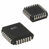
Micrel, Inc. 28-PIN PLCC (J28-1) MICREL, INC. 2180 FORTUNE DRIVE SAN JOSE, CA 95131 USA + 1 (408) 944-0800 TEL The information furnished by Micrel in this data sheet is believed to be accurate and reliable. However, no responsibility is ...

Related keywords