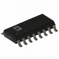
ADG451BRZ Analog Devices Inc, ADG451BRZ Datasheet - Page 12

ADG451BRZ
Manufacturer Part Number
ADG451BRZ
Description
IC SWITCH QUAD SPST 16SOIC
Manufacturer
Analog Devices Inc
Series
LC²MOSr
Type
Analog Switchr
Datasheet
1.ADG451BRUZ-REEL.pdf
(16 pages)
Specifications of ADG451BRZ
Function
Switch
Circuit
4 x SPST - NO
On-state Resistance
5 Ohm
Voltage Supply Source
Dual, Single, Dual Supply
Voltage - Supply, Single/dual (±)
±5V, 12V, ±15V
Current - Supply
0.5µA
Operating Temperature
-40°C ~ 85°C
Mounting Type
Surface Mount
Package / Case
16-SOIC (0.154", 3.90mm Width)
Analog Switch Type
SPST
No. Of Channels
4
On State Resistance Max
4ohm
Turn Off Time
60ns
Turn On Time
70ns
Supply Voltage Range
± 4.5V To ± 20V
Multiplexer Configuration
Quad SPST
Number Of Inputs
4
Number Of Outputs
4
Number Of Channels
4
Analog Switch On Resistance
12@±3.5VOhm
Analog Switch Turn On Time
220ns
Analog Switch Turn Off Time
160ns
Package Type
SOIC N
Power Supply Requirement
Single/Dual
Single Supply Voltage (min)
5V
Single Supply Voltage (typ)
9V
Single Supply Voltage (max)
12V
Dual Supply Voltage (min)
±5V
Dual Supply Voltage (typ)
±9/±12V
Dual Supply Voltage (max)
±15V
Power Dissipation
600mW
Supply Current
0.0005@±5VmA
Mounting
Surface Mount
Pin Count
16
Operating Temp Range
-40C to 85C
Operating Temperature Classification
Industrial
Lead Free Status / RoHS Status
Lead free / RoHS Compliant
Lead Free Status / RoHS Status
Lead free / RoHS Compliant, Lead free / RoHS Compliant
Available stocks
Company
Part Number
Manufacturer
Quantity
Price
Part Number:
ADG451BRZ
Manufacturer:
ADI/亚德诺
Quantity:
20 000
Company:
Part Number:
ADG451BRZ-REEL7
Manufacturer:
ENPIRION
Quantity:
2
Part Number:
ADG451BRZ-REEL7
Manufacturer:
ADI/亚德诺
Quantity:
20 000
ADG451/ADG452/ADG453
APPLICATIONS
Figure 15 illustrates a precise, fast, sample-and-hold circuit. An
AD845
amplifier is an AD711. During track mode, SW1 is closed, and
the output, V
SW1 is opened, and the signal is held by the hold capacitor, C
V
IN
AD845
is used as the input buffer, and the output operational
+15V
–15V
Figure 15. Fast, Accurate Sample-and-Hold Circuit
OUT
, follows the input signal, V
SW2
SW1
+15V
S
S
ADG451/
ADG452/
ADG453
13
5
–15V
+5V
12
4
D
D
75Ω
R
C
C
1000pF
C
2200pF
CH
2200pF
IN
. In hold mode,
AD711
+15V
–15V
V
OUT
Rev. C | Page 12 of 16
H
.
Due to switch and capacitor leakage, the voltage on the hold
capacitor decreases with time. The ADG451/ADG452/ADG453
minimize this droop due to their low leakage specifications. The
droop rate is further minimized by the use of a polystyrene
hold capacitor. The droop rate for the circuit shown is typically
30 μV/μs.
A second switch, SW2, which operates in parallel with SW1, is
included in this circuit to reduce pedestal error. Because both
switches are at the same potential, they have a differential effect
on the op amp, AD711, which minimizes charge injection
effects. Pedestal error is also reduced by the compensation
network, R
hold time glitch while optimizing the acquisition time. Using
the illustrated op amps and component values, the pedestal
error has a maximum value of 5 mV over the ±10 V input
range. Both the acquisition and settling times are 850 ns.
C
and C
C
. This compensation network reduces the


