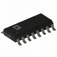
ADG451BRZ Analog Devices Inc, ADG451BRZ Datasheet - Page 4

ADG451BRZ
Manufacturer Part Number
ADG451BRZ
Description
IC SWITCH QUAD SPST 16SOIC
Manufacturer
Analog Devices Inc
Series
LC²MOSr
Type
Analog Switchr
Datasheet
1.ADG451BRUZ-REEL.pdf
(16 pages)
Specifications of ADG451BRZ
Function
Switch
Circuit
4 x SPST - NO
On-state Resistance
5 Ohm
Voltage Supply Source
Dual, Single, Dual Supply
Voltage - Supply, Single/dual (±)
±5V, 12V, ±15V
Current - Supply
0.5µA
Operating Temperature
-40°C ~ 85°C
Mounting Type
Surface Mount
Package / Case
16-SOIC (0.154", 3.90mm Width)
Analog Switch Type
SPST
No. Of Channels
4
On State Resistance Max
4ohm
Turn Off Time
60ns
Turn On Time
70ns
Supply Voltage Range
± 4.5V To ± 20V
Multiplexer Configuration
Quad SPST
Number Of Inputs
4
Number Of Outputs
4
Number Of Channels
4
Analog Switch On Resistance
12@±3.5VOhm
Analog Switch Turn On Time
220ns
Analog Switch Turn Off Time
160ns
Package Type
SOIC N
Power Supply Requirement
Single/Dual
Single Supply Voltage (min)
5V
Single Supply Voltage (typ)
9V
Single Supply Voltage (max)
12V
Dual Supply Voltage (min)
±5V
Dual Supply Voltage (typ)
±9/±12V
Dual Supply Voltage (max)
±15V
Power Dissipation
600mW
Supply Current
0.0005@±5VmA
Mounting
Surface Mount
Pin Count
16
Operating Temp Range
-40C to 85C
Operating Temperature Classification
Industrial
Lead Free Status / RoHS Status
Lead free / RoHS Compliant
Lead Free Status / RoHS Status
Lead free / RoHS Compliant, Lead free / RoHS Compliant
Available stocks
Company
Part Number
Manufacturer
Quantity
Price
Part Number:
ADG451BRZ
Manufacturer:
ADI/亚德诺
Quantity:
20 000
Company:
Part Number:
ADG451BRZ-REEL7
Manufacturer:
ENPIRION
Quantity:
2
Part Number:
ADG451BRZ-REEL7
Manufacturer:
ADI/亚德诺
Quantity:
20 000
ADG451/ADG452/ADG453
SPECIFICATIONS
15 V DUAL SUPPLY
V
Table 1.
Parameter
ANALOG SWITCH
LEAKAGE CURRENTS
DIGITAL INPUTS
DYNAMIC CHARACTERISTICS
POWER REQUIREMENTS
1
2
3
Temperature range for B version is −40°C to +85°C.
T
Guaranteed by design, not subject to production test.
DD
MAX
On Resistance Match Between Channels (ΔR
Analog Signal Range
On Resistance (R
On Resistance Flatness (R
Source Off Leakage, I
Drain Off Leakage, I
Channel On Leakage, I
Input High Voltage, V
Input Low Voltage, V
Input Current, I
t
t
Charge Injection
Off Isolation
Channel-to-Channel Crosstalk
C
C
C
I
I
I
I
Break-Before-Make Time Delay, t
DD
SS
L
GND
ON
OFF
S
D
D
= 15 V, V
, C
= 70°C.
(OFF)
(OFF)
3
S
(ON)
SS
= −15 V, V
INL
ON
or I
2
)
D
INL
S
INH
(OFF)
INH
(OFF)
D
, I
L
S
FLAT(ON)
= 5 V, GND = 0 V. All specifications T
(ON)
3
D
)
(ADG453 Only)
ON
)
25°C
4
5
0.1
0.5
0.2
0.5
±0.02
±0.5
±0.02
±0.5
±0.04
±1
0.005
70
180
60
140
15
5
20
30
65
−90
37
37
140
0.0001
0.5
0.0001
0.5
0.0001
0.5
0.0001
0.5
B Version
T
V
7
0.5
0.5
±2.5
±2.5
±5
2.4
0.8
±0.5
220
180
5
5
5
5
5
Rev. C | Page 4 of 16
MIN
SS
to V
to T
1
MIN
DD
MAX
to T
MAX
Unit
V
Ω typ
Ω max
Ω typ
Ω max
Ω typ
Ω max
nA typ
nA max
nA typ
nA max
nA typ
nA max
V min
V max
μA typ
μA max
ns typ
ns max
ns typ
ns max
ns typ
ns min
pC typ
pC max
dB typ
dB typ
pF typ
pF typ
pF typ
μA typ
μA max
μA typ
μA max
μA typ
μA max
μA typ
μA max
, unless otherwise noted.
Test Conditions/Comments
V
V
V
V
V
V
V
R
R
R
V
R
R
f = 1 MHz
f = 1 MHz
f = 1 MHz
V
D
D
D
D
D
D
IN
L
L
L
S
L
L
DD
= 300 Ω, C
= 300 Ω, C
= 300 Ω, C
= 50 Ω, C
= 50 Ω, C
= 0 V, R
= −10 V to +10 V, I
= ±10 V, I
= −5 V, 0 V, +5 V, I
= ±10 V, V
= ±10 V, V
= V
= V
= 16.5 V, V
S
INL
= ±10 V; see Figure 18
or V
S
= 0 Ω, C
L
L
S
S
S
INH
L
L
L
= 5 pF, f = 1 MHz; see Figure 22
= 5 pF, f = 1 MHz; see Figure
= −10 mA
= ±10 V; see Figure 17
= ±10 V; see Figure 17
SS
= 35 pF, V
= 35 pF, V
= 35 pF, V
; all others = 2.4 V or 0.8 V, respectively
= −16.5 V; digital inputs = 0 V or 5 V
L
S
= 1.0 nF; see Figure 21
S
= −10 mA
= −10 mA
S
S
S1
= ±10 V; see Figure 19
= ±10 V; see Figure 19
= V
S2
= +10 V; see Figure 20
23


